Hi team,
i got a question from customer. The question is listed below. Could you please help to comment it. Thanks.
I met a question in AWR1642 RF PCB design.
I found 2 file in TI offcial website, one is named"TI mmWave Radar sensor RF PCB Design, Manufacturing
and Validation Guide", the other is named "HardwareDesignChecklist_V0p7_AWR1642_SWRR154".
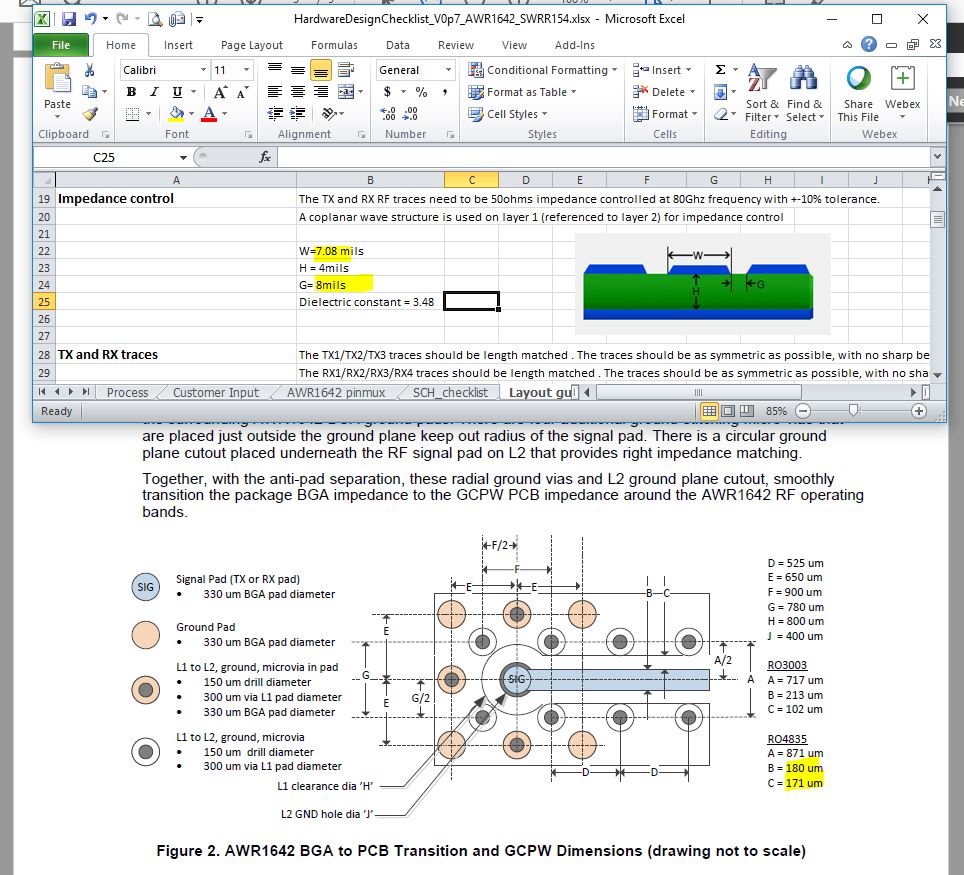
In "TI mmWave Radar sensor RF PCB Design, Manufacturing and Validation Guide", it recommed the RF
PCB as below, width of RF trace is 7.08mil ,gap is 6.73mil(171um).PCB material is RO4835.
But in HardwareDesignChecklist, it gives a different design that is width of RF trace is 7.08mil ,gap is 8.0mil. PCB stackup is the same as above.
Can you kindly the me what are the reasons or which is right? Thank you very much.