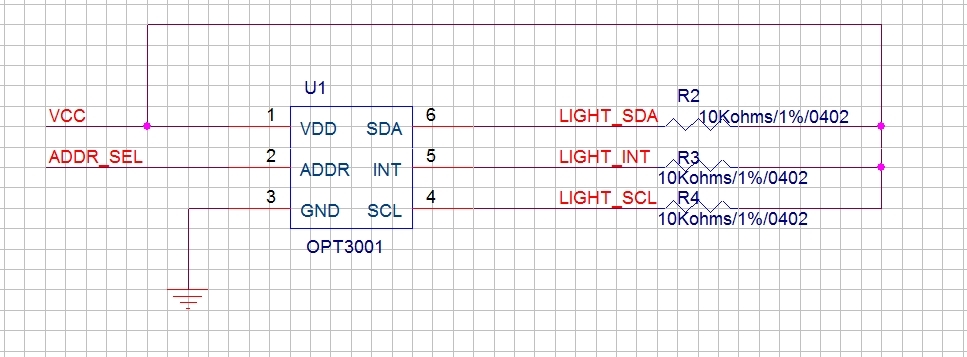
 My customer is using OPT3001 in OLED screen. Here is the Schematic diagram.
They want to know answers below:
1. Is it OK? I know that 100nF bypass capacitor is absent.
2. Where does AADR pin need to connect? Could it be dummy?
This thread has been locked.
If you have a related question, please click the "Ask a related question" button in the top right corner. The newly created question will be automatically linked to this question.
 My customer is using OPT3001 in OLED screen. Here is the Schematic diagram.
They want to know answers below:
1. Is it OK? I know that 100nF bypass capacitor is absent.
2. Where does AADR pin need to connect? Could it be dummy?