This thread has been locked.

If you have a related question, please click the "Ask a related question" button in the top right corner. The newly created question will be automatically linked to this question.

PGA302: Question for PGA302, PGA305, PGA900

Part Number: PGA302
Other Parts Discussed in Thread: PGA900, PGA305

Hi professional,

Our customer has questions for PGA302, PGA305, PGA900.

1.PGA302

  • As datasheet mentioned, Output sample rate is typ 96us. is this meaning that ADC's sample rate is 96us?
  • this specification's test condition was written "Sample period control bit = 0b00". However I couldn't find "Sample period control bit" on the other page. What is "Sample period control bit"?
  • Is the actual output rate determined by decimation filter setting?
  • Which register can set the decimation filter?
  • Simplified Block Diagram has I2C block. But Functional Block Diagram don't has I2C. Could you explain about constitution of I2C block?
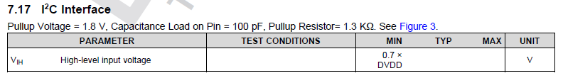
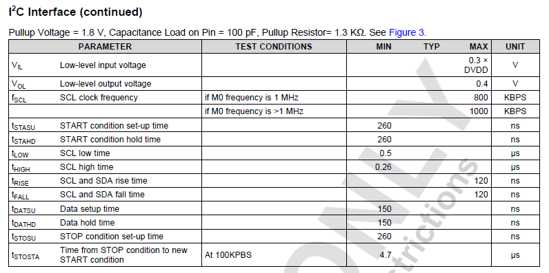
  • I couldn't found specification for I2C interface(i.e. data rate). Could you provide it?

2.PGA305

  • The datasheet said that "Output rate" is "Typ 512us" in the "Operating Characteristics". however this said "a 16-bit ADC at a 7.8-kHz(128us) output rate" in 7.1 Overview. So this  description make confusion for me. Would you explain about meaning of Output rate and why this device has 2 type of output rate? By the way My understanding of response time is that the time from the input of the signal to the output of the data.  is this correct?

3.PGA900

  • In the case of PGA900 datasheet Output sample period on Operating Characteristics is 64us or 128us. And Output rates on "7.1. Overview" is 7.8kHz(128us) or 15.6kHz(64us). Do these mean the same thing?
  • Are the meaning "Output sample period" and "Output rate" ADC's sample rate?
  • Dose "Sample period control bit" same as "PADC_ DECI_RATE"?

4.General question

  • PGA302, PGA305 and PGA900 looks like similar products. However they use various terms and definitions.(i.e. Output rate, Output sample period) So our customer guessed there product has big difference. thus their datasheet used various terms and definitions. Is this correct? or is this just orthographical variants?

I'm looking forward hearing from you.

Best Regards,

Kazuki Kuramochi

  • Hello Kazuki,

    1. PGA302
    -This is the time it takes between when the ADC codes are available from the ADC
    -This is an internal control that is not available to the user in the PGA302. There is only one available sample output rate
    -Yes this is the decimation filter output rate. I realize that the datasheet mentions there is more than one selectable rate, but in the PGA302 the only available output rate is a fixed 96us
    -There is no register to set the decimation filter output rate
    -It is a standard I2C block for an I2C slave device
    -The I2C specifications should be there. I will have to look into this

    2. PGA305
    -The output rate of 512us from the specification table is the total output time from input to analog output on VOUT. The ADC decimation output time is the 128us from section 7.1

    3. PGA900
    -Yes they mean the same thing
    -No, these are not the ADC's sample rate. It is a delta-sigma ADC which oversamples. The output rate and output sample period are the output rate of the decimation filter
    -Yes, the output period control is the PADC_DECI_RATE bits

    4.
    The overall function of the devices is similar. The differences in some of the terms that refer to the same thing are just incidental.

    Regards,
  • Hello Scott,

    Thank you for your answer for my questions.
    I have additional question for your answers.

    1.PGA302
    ・You mentioned PGA302 has fixed output rate. Is this meaning that the datasheet 8.3.10.2(Can be configured 96us, 128us,...) is wrong. Is this understanding correct?
    ・I want to know about the detailed internally connection of I2C. Simply put, Does same as PGA305 block diagram on Chapter 7.2 of PGA305 Datasheet?
    ・I couldn't found the interface specification of I2C(i.e. communication rate) on datasheet chapter 8.3.15.2 and 8.3.15.3. Would you explain this points?

    2.PGA305
    ・Could you describe about Response time and the difference between Output rate and response time?

    I'm a waiting your reply.

    Best regards,
    Kazuki Kuramochi
  • Hello Scott,

    Would you provide you answer for my questions?

    Best regards,
    Kazuki Kuramochi
  • Hello,

    PGA302

    • Yes, it has a fixed output rate. That is a mistake in the datasheet.
    • The PGA305 datasheet block diagram showing the I2C connections internally is not very detailed. It is a basic block that shows the SDA, SCL, and ADDRESS pins coming out of the device. In the PGA302, the connections are similar. There isn't more detail that can be gone into without revealing the actual design schematics
    • As I mentioned in my previous post the I2C specifications are not in the datasheet, but they should be there. I am looking into getting this fixed

    PGA305

    • The output rate is the time from the analog input change, to when the output begins to change. The Response Time is the time from when the analog input changes to when the output has completely settled at 90% of its new value. 

    Regards,

  • Hello Scott,

    Thank you for your kind explanation.
    I understood.
    If we have new question for these product, I will as you.

    Best regards,
    Kazuki Kuramochi
  • Part Number: PGA302

    Hello professional,

    My customer has 2 questions PGA305 I2C block.

    1. I posted question for PGAxxx series product under this E2E thread. In this thread, Scott said PGA305's I2C block is same as PGA302. However datasheet's function block diagram of PGA305 is different from PGA302. Is this just mistake?

    2. In prior E2E thread, Scott mentioned he will revised datasheet regarding I2C setting. Would you provide when do you release fixed datasheet. If it is difficult, could you provide the setting parameter of I2C? (baudrate, etc...)

    I'm looking forward hearing back from your.

    Best regards,

    Kazuki Kuramochi

  • Hello Kazuki,

    I have joined your new post with the original thread since there is no new question being discussed.

    1. I did not say that the PGA305 and the PGA302 have the same I2C block. They have similar functionality, so I referred you to look at that. The overall functional block diagram is very different because these are entirely separate devices.

    2. We do not have a set timeline on when this will be updated. There are many document updates waiting in the queue. 

    Below are unofficial specifications from a draft datasheet update.

    Regards,

  • Hello Scott,

    Thank you for providing I2C specification.

    Sorry for my miss understanding regarding I2C.
    Then, Why isn't there I2C signal line on the PGA302 Functional Block diagram?
    Our customer would like to know the reason of missing I2C line on functional block diagram of PGA302 in spite of there is I2C line on simplified block diagram of PGA302, 305 and functional block diagram of PGA305.
    Both simplified block diagram is similar regarding communication line. However there isn't I2C line on PGA302's functional block diagram.

    Best regards,
    Kazuki Kuramochi
  • Hi Kazuki,

    Thank you for the explanation. I see the confusion now. I2C is a part of the device, but it is not currently not shown in the Functional Block Diagram in the datasheet. This is something that needs to be updated, and it will be addressed in the next revision of the datasheet.

    Regards,