Other Parts Discussed in Thread: AWR1642,
I refer to the above information available in the excel sheet " Hardware design checklist - swrr154.xlsx"
The following statement in quotes is taken from the same document
"The layer one is referenced to Layer2 GND. There should be continuous GND planes on the Layer 2 below the RF traces. ONLY below the RF balls in the AWR1642 device the L2 layer has a 15.8mil diameter opening. Below this opening the Layer 3 should be solid GND"
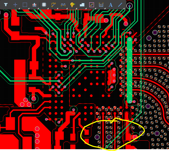
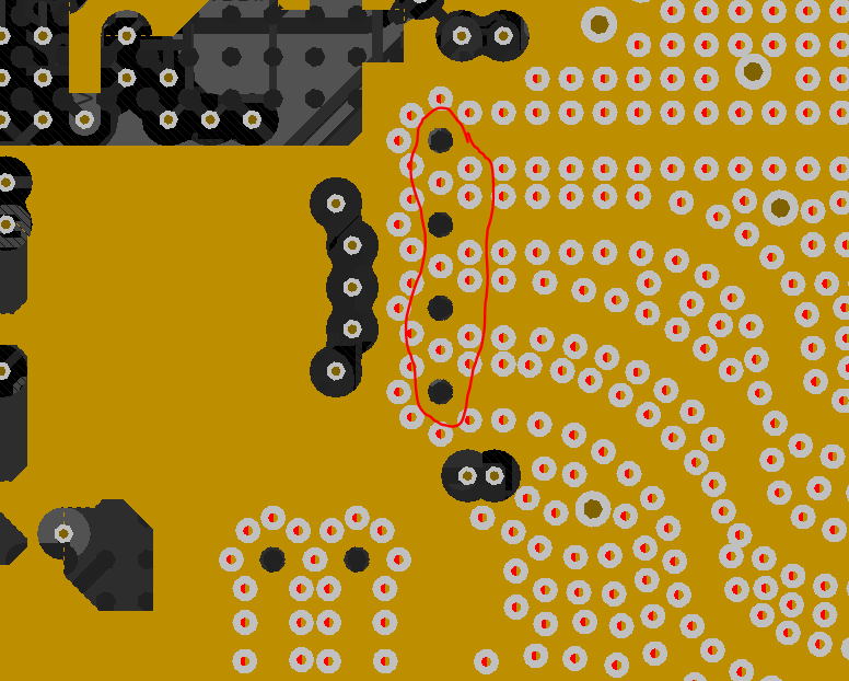
I refer to the TIDA020011 design , the layer 3 area below these openings, is not a solid GND plane but seems to be power. The layer 3 area below the RF holes are as below
can you confirm whether the highlighted text is a typographical error or is Layer 3 should be a solid ground below that area.
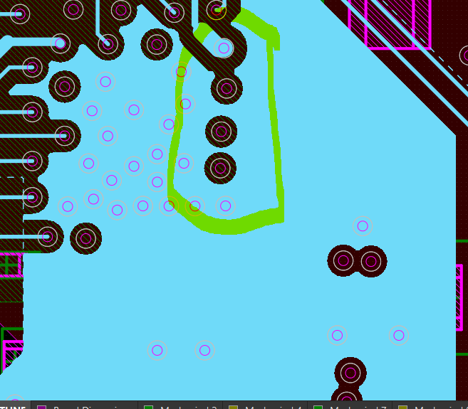
I looked at the AWR1642BOOST-ODS evm design files- it appears to have a ground plane in layer 3 as well.

Can some one confirm how important is this Layer 3 ground for the antenna range performance. I am looking for the same antenna performance as that of the ODS which has a 15m range.
Can some one also confirm whether the TIDA020011 board has a range of 15m - this will resolve my query in unequivocal terms.