Hello;
Hello;
Is it a good choice or bad choice surround fdc and LC component with ground plane When using single ended sensor confuguration.
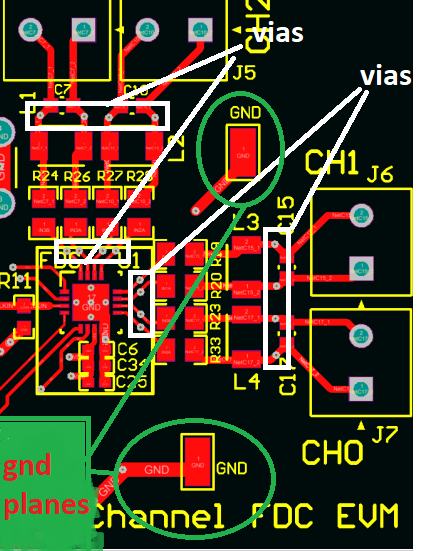
1-what is the side effect of ground plane which is surround LC tank?
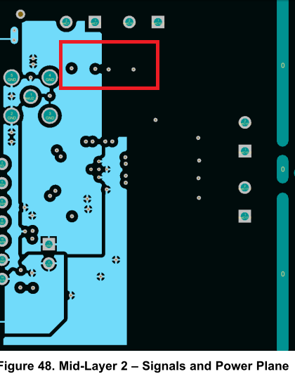
2-Ground plane is not drawn bottom and top layer on FDCEWM, it is drawn mid-layer1 and mid-layer 2. WHY? is there any reason?
3-There are two GND plane which are in green circle. what is the purpose of them? and how many distence must be between LC and gnd plane?
4- There are power plane around capacitance input pins, as you see below picture. What is effect of this?
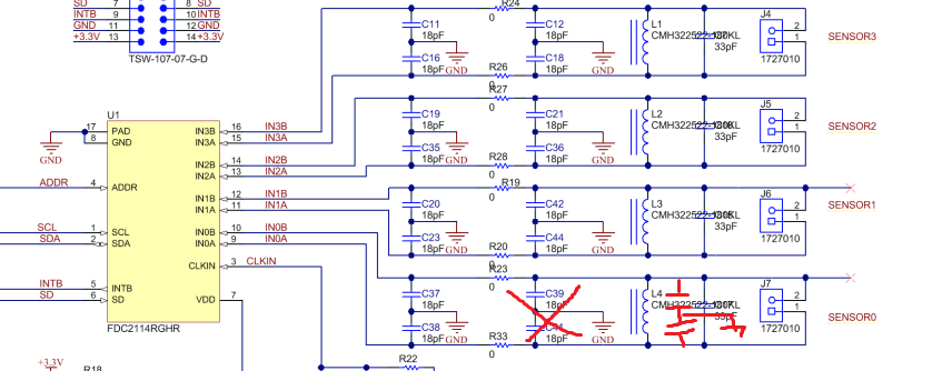
5- There is some capacitor for emi reduction. For example C39, C41. The caps connected between L and C on layout. But on shematic they connected betweeen CMC and L.
In teoricaly they connected in paralel in two ways. But is there any advantages(noise reduction) to connect them between L and C.
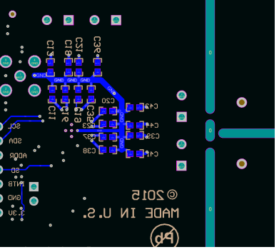
6- Below picture is bottom layer. Noise reduction capacitor is on bottom layer. why?
Is the reason keeping away ground from LC?
Best Regards


