Because of the holidays, TI E2E™ design support forum responses will be delayed from Dec. 25 through Jan. 2. Thank you for your patience.

This thread has been locked.

If you have a related question, please click the "Ask a related question" button in the top right corner. The newly created question will be automatically linked to this question.

FDC2214EVM: I2C controller for FDC2214

Part Number: FDC2214EVM
Other Parts Discussed in Thread: FDC2214, , FDC1004EVM, FDC1004, FDC2212, MSP430F5529, LDC1614EVM, LDC1614, OPA322

Hi,

I am going to use LabVIEW to control the FDC2214, however, TI does not have LabVIEW support for FDC2214, alternatively, I am going to use National Instruments(NI)  I2C module NI USB-8452. 

The NI USB-8452 is a USB 2.0 high-speed, high-power device with a maximum theoretical transfer rate of 480 Mb/s. Using a high-speed FPGA-based architecture, the NI USB-8452 supports SPI data acquisition up to 50 MHz and I2C communication up to 3.3 MHz. The programmable reference voltage covers logic families from 1.2 V to 3.3 V, which makes the NI USB-8452 versatile for most SPI/I2C tests and verifications.http://www.ni.com/pdf/manuals/371746d.pdf

The FDC2214 has a frequency requirement in both master clock (2-40MHz) and excitation (0.01-10Mhz). The up to 3.3Mhz frequency limit of the NI USB-8452 is at the very low end of the FDC2214. 

I would like to know if the NI USB-8452 can be used to control the FDC2214. The benefit of using a NI I2C controller is that NI provide many VIs and descriptions on how to use the VIs, which make it easier for me to program the controller according to my application.

Regards,

Gu


  • Hello Gu,

    You may use the NI USB-8452 to control the FDC2214 as long as you do not exceed the maximum I2C clock frequency of 400kHz.

    I do not recommend using the 3.3MHz clock for CLKIN, which is the first frequency requirement you mentioned. Your resolution will be much better with higher reference frequencies. Use the 40MHz external clock on the FDC2214EVM if possible.

    The excitation frequency you mentioned is not influenced by CLKIN or the I2C clock frequency. The FDC2214 can drive sensor frequencies in this range regardless of the CLKIN and I2C clock frequencies.

    Best Regards,
  • Hi Kristin,

     Thank you for your reply.

    The FDC 2214EVM uses MSP430 as its controller, I did a search for MSP430 on your web and could not find a link that specifically for MSP430, all  results are MSP430 with other component., e.g. FDC1004EVM (=MSP430+FDC1004). Could you please provide a link or a document that has information in details on the controller itself.

    I first like to know if a MSP430 can handle multiple FDC2214s (or FDC2212s)? how many if it can?

    Is there any difference in accuracy and sample rate between FDC2214 and FDC2212 if only one channel is used? 

    I am thinking to use only one channel at its highest sample rate and then make a moving average to increase data precision. And use multiple boards to make multiple (4-8) channels. 

    Regards,

    Gu


  • Hi Gu,

    The FDC2214EVM uses the MSP430F5529 MCU, which you can find more information about here: www.ti.com/.../MSP430F5529

    The MSP430 (or any MCU) can control up to two FDC221x devices on the same I2C bus. This is because the FDC221x has only two I2C address options, controlled by tying the ADDR high or low. If you need more than two FDC221x devices controlled by a single MCU, you would need to use an I2C expander.

    No, there would be no difference in sample rate for single channel continuous measurements using the FDC2212 and the FDC2214. There would be a difference between the FDC221x and the FDC211x sample rate and accuracy, because the FDC211x is lower resolution and can support faster sample rates.

    What is your application? The moving average may or may not be a good idea depending on your application.

    Best Regards,
  • Hi Kristin,

    My application need 4-16 differential sensors, all are relative

    measurement, so precision is more important than accuracy, the higher

    precision the better for my application, preferably ±0.0001pF.

    The best option is to use 1-4 of FDC2214 with a MSP430 plus an I2C

    expander. However, I am not good at C, hence I have difficulty to

    program MSP430. I am comfortable to use Labview. It would be better if

    you have labview support for FDC2214/2212. Using NI USB8452 is my

    alternative option only.

    Based on the FDC2214 datasheet, an active driven shield can improve

    measurement precision,which is used by FDC1004. However, I am still not

    clear how to make an active driven shield for FDC 2214/2212. Could you

    please provide some additional information on this shielding application?

    Moving average is one type of digital filters, labview has many digital

    filter function VIs available. I can try different filters once data is

    read into a buffer.

    Using 4 channels on each FDC2214 can reduce cost and have a smaller

    footprint, but the wire length from each sensor to input channel on the

    PCB will have to be different, which creates different paradise

    capacitance. To minimize difference in paradise capacitance  between the

    sensors, it might be beneficial to use only one channel of a PCB for one

    differential sensor, so that the PCB can be mounted as close as possible

    and the same length wire to the sensor. this also makes its aggregate

    sample rate for single channel use, collecting more data for digital

    filtering.

    These are my thoughts.  I might be wrong. Please feel free to advise.

    Regards,

    Gu

  • Hello Gu,

    Unfortunately we do not have Labview code available for the FDC devices. We do have the FDC2214EVM firmware source code available with the GUI download. In addition, we also have this sample code for communicating directly with the MSP430 on the LDC1614EVM. The LDC1614 uses the same I2C protocol as the FDC2214, so it should be simple to adapt the code to controlling the FDC2214. The MSP430 is the same on both EVMs. 

    It sounds like your application is somewhat similar to the approach we use for touch-on-metal inductive sensing. In this TI Design, we use a moving average to implement a baseline tracking function. This compensates for environmental shifts. The design guide includes information about the baseline tracking algorithm. 

    I'll note that your desired resolution is extremely small. This shift in capacitance translates to a very small change in sensor frequency (roughly 0.1Hz to 10Hz from some basic calculations). While this is technically measurable with the FDC2214, which has an LSB of <1Hz, it is very unlikely that your noise floor would be low enough to make accurate measurements at this resolution.

    As for the active shield, you should use an op amp configured to be a buffer for either the INxA or the INxB signal, which will be the shield. This thread may help you further.

    If your sensor is in an area where the parasitic capacitances will be stable, I do not think you need to worry about differences in wire length. The exact sensor frequency does not matter; only the change in sensor frequency matters. If the parasitic capacitances can change, shielding the wires would be more important than matching the lengths. Note that there is a maximum distance that the sensor can be separated from the FDC2214. This maximum distance is based on the sensor frequency. If you need to use long wires or cables, choose your inductor so that the sensor frequency is under 1MHz.

    Best Regards,

  • Hi Kristin,

    Thank you for your very informative reply.

    Due to the fact that I need the extreme  high precision, I  have to take all possible measures for noise reduction. I have 2 major questions for you.

    1. In terms of actively driven shielding, your suggested an operational amplifier  (OPAx322). OPAX322 is for signal conditioning for either INxA or INxB of FDC2214, which is different from the actively driven shielding used in FDC1004. FDC1004 has 2 inputs, SHLD1 and SHLD2, for shielding. (1) Do the shielding and signal conditioning play the same role in using the FDCs?  (2)Can the populated +5V (beside Y1, the oscillator for MSP430) or +3.3V (beside J8) on the FDC2214EVM be used for OPAX322? OPAX322 accepts up to 6 V power supply.

    2. In terms of using MSP430 to control multiple FDC2214/2212, you mentioned that MSP430 can handle 2 FDC2214/2212 and needs an expender for more than 2 FDC2214/2212s application. I went through the MSP430 user guide (SLAU208Q) and my understanding is that MSP430 can handle 2 I2C as masters and each I2C master can handle many I2C as slaves (see page 997). I may use one SMP430 to control up to 8 FDC2214/2212s.  Could you please check the doc to see if my understanding is correct?   Also please specify the maximum number of FDC2214/2212 can be used with a SMP430 without using an external power supply? I noticed that each FDC2214/2212 consumes 2.1mA at active status. What is the maximum current draw allowed from a SMP430? and what external power supply can you recommend if an external one must be used?

    Thanks,

    Gu    

  • Hi Gu,

    My apologies for the delayed reply.

    1. The shielding principles are approximately the same, but as you noted the FDC2214 does not have an integrated shield driver. This is why it is necessary to use an external amplifier. I do not suggest using the +5V or +3.3V power supplies on the board, because the op amp needs to be able to output 0V (which it can't do if its negative supply is also 0V). I suggest using an external power supply for prototyping.

    2. I am not an MSP430 expert, so I suggest posting a new E2E thread that the MSP430 team can answer. For the I2C question, let them know that the key limitation for the FDC221x devices is that there are only two possible I2C addresses.

    Best Regards,
  • Hi Kristin,

    Thank you for your reply.
    As for using OPAX322 to condition FDC2214 input signal, I do not understand that it needs to be able to output 0V. It has an unit gain. My understanding is that it just outputs the imputed-voltage or the excitation voltage. Could you please elaborate a bit for me to understand it?

    For the MSP430 controller issue, I have posted a new question on MSP430 forum.

    Best regards,
    Gu
  • Hello Gu,

    My apologies for the delayed reply; I was out of office on business travel. 

    If you look at the INxA/INxB signals, you will see a half-wave rectified sine. The signals are 180 degrees out of phase with each other, and when one pin is supplied a sine wave the other pin is grounded. 

    Because the excitation voltage reaches 0V, the op amp must also be able to supply 0V. All op amps (even rail-to-rail output op amps) have an output swing that does not quite reach the supply rails (specified in the datasheet). An op amp with a negative rail of 0V will only be able to output 0V plus the specified output swing. If this is unclear to you we have some videos that should help: https://training.ti.com/ti-precision-labs-op-amps . See Section 3: Input and Output Limitations.

    If the output voltage of the op amp is a few millivolts when it should be ground, there will be additional capacitance between the buffered signal and the original INxA signal, which is not ideal. Using a negative supply rail for the op amp allows it to output 0V and prevent this issue.

    Best Regards,

  • Hi Kristin,

    I really appreciate your efforts in helping me with the issues. 

    I do not have an oscillator to see the waveform. 

    As for using OPA322 as an actively driven shield or front signal conditioning, I run into issues and had posted it on the forum.

    e2e.ti.com/.../2994624

    Could you please have a look and give me some suggestions?

    Regards,

    Gu

  • Hi Gu,

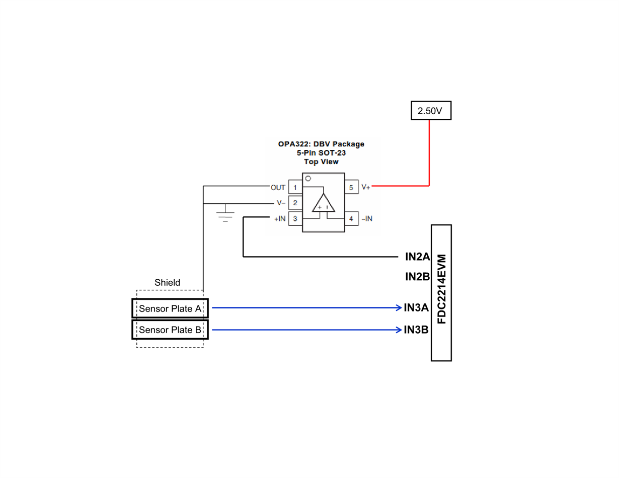
    I'd be happy to help you further with the op amp circuit. Give me a couple of days so I can draw a suggested circuit for you. In the meantime, I think that it may have been unclear where to place the op amp. You do not want it to interfere with the FDC properly driving the LC tank, so it should not be in series with your sensor. Instead it should be in parallel with the sensor, and you will need an additional conductive plate at the output of the op amp to act as the shield.

    Best Regards,

  • Hi Kristin,

    Thanks, take your time. 

    Gu

  • Hi Gu,

    Try this circuit: http://www.ti.com/lit/an/sboa269a/sboa269a.pdf

    Connect either IN0A or IN0B to the positive amplifier input. Make sure that the amplifier is in parallel with the LC tank. For the OPA322, do not use +/-15V supplies. Instead use +/- 2.5V supplies. Connect whatever conductive shield (like a piece of copper tape) to the output of the amplifier.

    I hope this helps!

    Best Regards,

  • Hi Kristin,

    I am including a drawing, could you please take a look and let me know whether I understood it correctly?

    Regards,

    Gu

  • Hi Gu,

    That's not what I meant. I've drawn a picture that should help.

    Note that the copper shield plate should not be directly connected to the FDC2214. It should only be connected to the output of the amplifier. It should be the same size as the sensor plate you are using to detect changes in capacitance and should be located very close to the sensor plate.

    Best Regards,

  • Hi Kristin,

    Thanks, I will try it out soon. I have to buy a +/- 2.5V power supply for the try.

    Best regards,

    Gu