This thread has been locked.

If you have a related question, please click the "Ask a related question" button in the top right corner. The newly created question will be automatically linked to this question.

TDC7200EVM: Split INTB pin output (Interrupt) and feed it to two boards.

Part Number: TDC7200EVM
Other Parts Discussed in Thread: TDC7200

I'm using TDC7200EVM with Arduino uno. I'm feeding external Start, Stop and clock from my setup. I  require the Interrupt (INTB pin) output at both the Arduino board and an FPGA board. Hence I attempted to split the INTB pin output (which is active low) using a voltage divider, but it did not work.

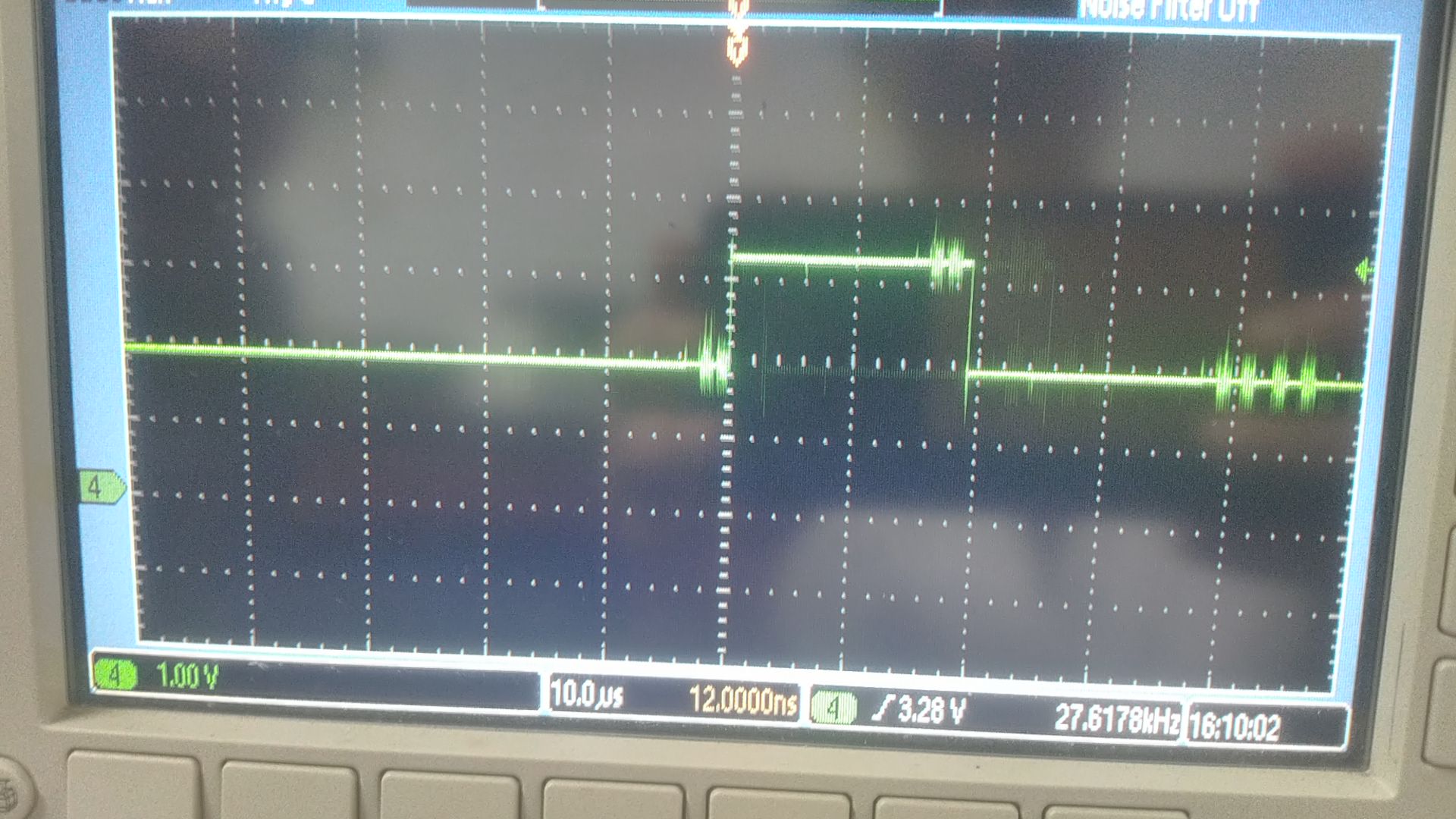
When I measure the INTB output without giving start and stop signal in an oscilloscope I see a 3.2V DC signal.When I feed external start and stop signals, the voltage reduces to 19mV (which i checked using multi-meter, as i was unable to measure on oscilloscope).

How do I split the INTB pin output, so that I can feed the signal to two boards?

  • Foram,

    Please let me know why you send the INTB signal to both the MCU & FPGA board.

    The INTB pin is typically High and goes low when the measurement cycle is complete. The TRIGG pin also helps to let us know if a particular cycle of measurement is complete.

    You can use the TRIGG pin as well to know if a particular measurement cycle is complete. Try to connect the TRIGG pin to FPGA & the INTB pin to the MCU.

    Also note that INTB pin is active low open drain.

  • TRIGG pin when viewed on oscilloscope seems to have more noise compared to the INTB pin. So we used a voltage divider with two 100 kohm resistors and reduced 3.2V to 1.5V (as FPGA can accept max 2V(LVCMOS)). 

    Now my interrupt pin shows 1V DC with 0.5V peak pulses (1.5V peak to peak) at time period of 680micro seconds , directly when I make continuous measurement from TDC7200 IC, when am trying to measure TOF between 32ns pulse and 64ns pulse (%50 duty cycle).   I've attached a screenshot of the INTB output signal.

    Kindly advice If this is correct? why is there a 1V DC in the INTB output signal.

  • To split the INTB to MCU and FPGA  we used a voltage divider with two 100 kohm resistors and reduced 3.2V to 1.5V (as FPGA can accept max 2V(LVCMOS)), but this did not work as well.  And now we see a 1V DC in the INTB output signal as described above.

    What Logical level is the INTB pin? is it TTL?

  • Foram,

    I will get back you on these questions by tomorrow.

  • Foram,

    INTB pin is a output pin from the TDC7200 device and incase you want to use send this signal to FPGA and MCU you should be able to do so without any issues. However if your FPGA cannot accept the current voltage level of the TDC7200 output you should be able to find a level shift IC and translate it to the device.