This thread has been locked.

If you have a related question, please click the "Ask a related question" button in the top right corner. The newly created question will be automatically linked to this question.

TMP112: TPM112, How can the temperature sensing area contact the hot body better?

Part Number: TMP112
Other Parts Discussed in Thread: TMP117, HDC1080, HDC2080

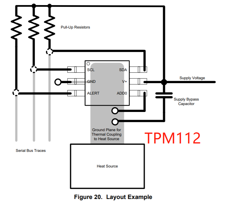
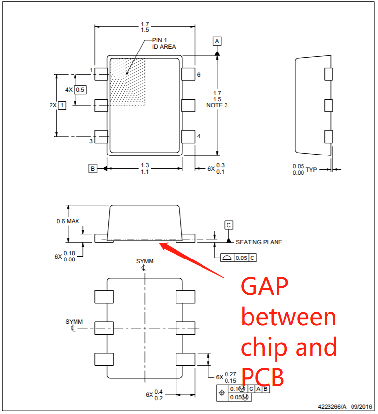
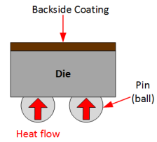
From this picture, it seems that the temperature sensing area of TPM112 is at the bottom of the chip. But from the chip structure, there will be a gap between the bottom of the chip and the PCB. How can the temperature sensing area contact the hot body better? Thank you very much.

  • Hi Xiansheng,

    Thanks for your question.

    Section 6.4 gives the thermal information for the TMP112 in the SOT563 package. We recommend sensing in this way because the thermal resistance between the junction and board is the smallest value. This is because the device pins (in the example layout GND), conduct heat to the die more effectively than the package compound.

    So for example, you could use the top side of the device to make contact with a heat sink, provided there is enough thermal isolation between the device pins and other heat sources. This will affect thermal response time, as it takes slightly longer for the device to absorb heat through the top side than through the pins, but with enough isolation this will not be critical. For more information on the primary conduction paths of various packages, you can check this application note.

    If you wanted to use bottom side sensing, then I would recommend exposing the copper GND plane on the bottom side, which can then be attached to a bio compatible material such as stainless steel, which would make actual contact with the skin.

    Let me know if you have any other questions. 

    Best Regards,
    Brandon Fisher

  • Thank you Brandon  ,

    It is helpful.  could you please, one more question , like TMP112, all pins are connected to Die through Bond Wire or just which one? and how about HDC1080  and  TMP117 , all pins or which one ?

    thanks a lot !

  • Hi Xiansheng,

    All pins on the TMP112 will be connected via bondwire to the die. The same is true for the DRV (WSON) package of the TMP117 and the HDC1080. However the thermal pads for the TMP117 (DRV) & HDC1080 are connected directly to the die using an epoxy, and will end up being the more dominant thermal path. Keep in mind that the TMP117 thermal pad should not be soldered down, and for the HDC1080 you should not connect the device pad to GND (it can be soldered to a floating pad). If you're interested in humidity sensing as well, I recommend taking a look at the HDC2080 device as well. 


    As I mentioned in the other thread, there is also a DSBGA package for the TMP117 which is almost a bare die. In this case there is little thermal resistance between the top side of the device and the die, and between the solder balls and the die. 


    Your biggest tool in controlling your thermal path however is space. In general, if you want to sense something specific, place your sensor close to the object you want to sense, and farther from other heat sources such as MCUs or FETs. If you want to use the GND pin to be the primary path, place the ground pad its connected to and the via close to the device, and put the sensor further away from devices that draw more power. 

    You can also use PCB cut-outs to further isolate the sensor from the rest of the board. 

    Best Regards,
    Brandon Fisher