- Ask a related questionWhat is a related question?A related question is a question created from another question. When the related question is created, it will be automatically linked to the original question.
Original question:

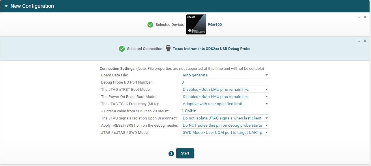
CCS/PGA900: How to down load firmware to PGA900 OTP by XDS200?
Hi.
I try to use uniflash to program OTP of PGA900. But I meet problem now.
Just like the picture, I can load and verity .hex file and read memory . But the setting page is blank. I can't flash OTP.
The PGA900 OTP is still blank after load .hex file.
Could you tell me how to use unifalsh to program OTP of PGA900?