This thread has been locked.

If you have a related question, please click the "Ask a related question" button in the top right corner. The newly created question will be automatically linked to this question.

Compiler/AWR1243BOOST: AWR1243BOOST

Part Number: AWR1243BOOST
Other Parts Discussed in Thread: AWR1243

Tool/software: TI C/C++ Compiler

Hello,

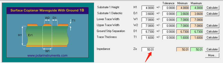
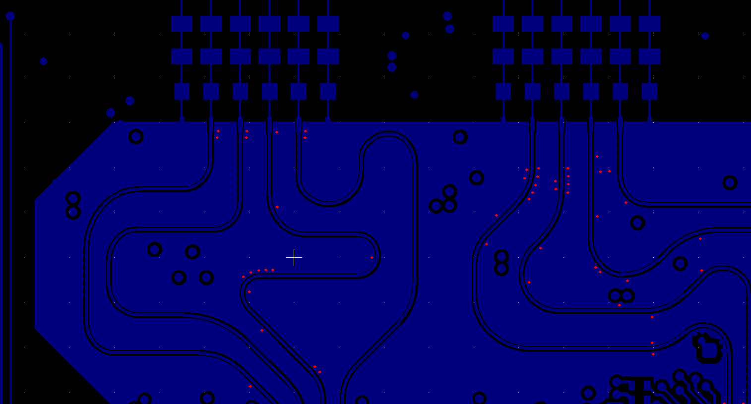
I have a problem about AWR1243 PCB layout. I see in AWR1243BOOST PCB, there are many blind holes around transmitting and receiving antennas from top to layer2. Because the process of blind hole is very expensive,  I want to konw if I can use the through hole to replace the blind hole, if it can not , why?

is it possible if all layers under the antenna area are paved GND or keep empty, Is this workable to use the through hole? Can you give me some advice? thanks very much!

  • Hello ,

    The GND vias around the RF traces are mainly for impedance control and shielding. The blind vias allow routing to be done in other layers and also closer spaced vias because the diameter is smaller. But as such you can use through hole vias as well, you just need to simulate the trace impedance with the vias you place.

    Regards,

    Vivek

  • Hello, Vivek

    Thanks for your reply, I don't  fully understand what you last sentence. I use polar Si9000 compute 50ohm waveguide strips, as follows

    The impedance information I calculated based on the parameters of AWR1243BOOST, but it does not involve the diameter and spacing of the via around the TR antenna.

    So, how can I simulate the trace impedance with the vias? What tools are used to simulate trace impedance with the vias? 

    in addition, I see in mmWave Cascade Radar RF Board (four AWR1243P cascade), The blind vias around TR antenna of  Cascade Radar RF Board are not as dense as those around AWR1243BOOST,

    The blind vias in Cascade Radar RF Board  are shown below in the red dots, Why this RF Board does not need many continuous via around the TR antenna?

    Thanks very much. 


  • Hello,

    You can use EM simulation tools like HFSS to simulate the impedance with the board layout. At 80Ghz the polar calculator may not be accurate.

    Regarding the via spacing on the cascade RF board, the image you shared does not seem to be enabling the 1-2 vias. Below is the image of the cascade RF board. You can see that the 1-2 GND vias are very closely spaced all along the RF trace.

    Regards,

    Vivek