This thread has been locked.

If you have a related question, please click the "Ask a related question" button in the top right corner. The newly created question will be automatically linked to this question.

LDC2112: LDC 2112 detect distance、material、coil design

Part Number: LDC2112
Other Parts Discussed in Thread: LDC2114

Hi 

I have a few questions as below, please advise.

thanks.

1. If we use glass materials, does FPC need to add strain relief?

2. What is the minimum distance from the main board under the coil?

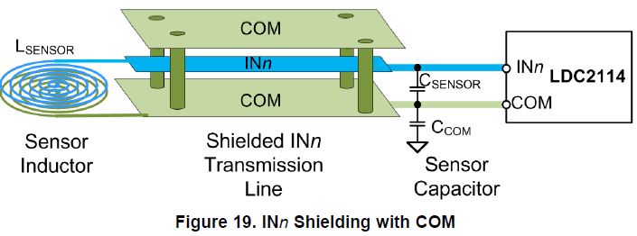
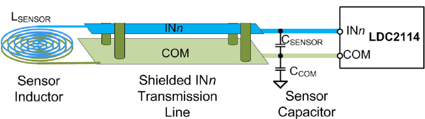
3. Does INn need the ground to cover the upper and lower layers?

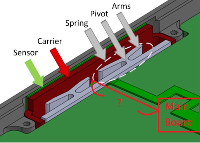
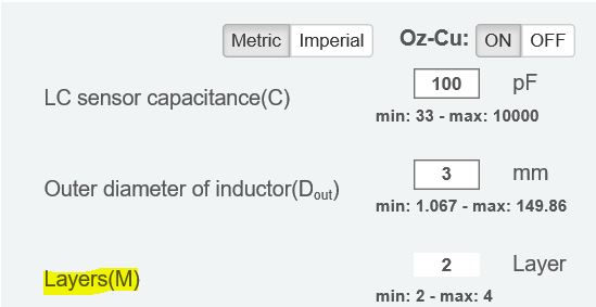
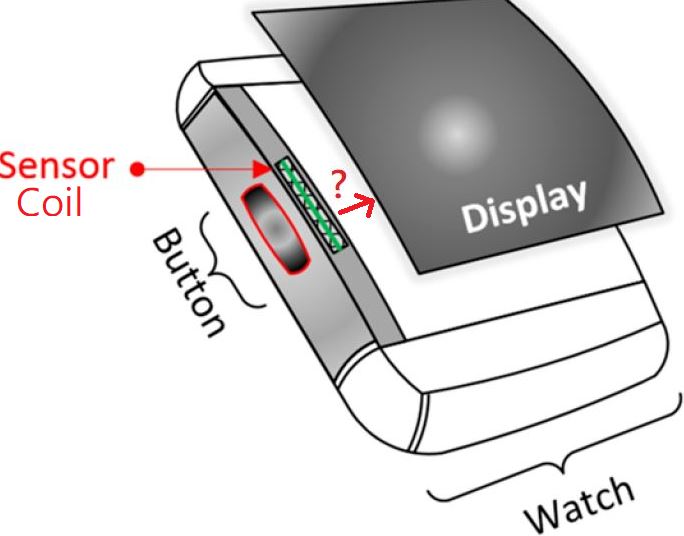
4. what is the detect distance as below pic? what is the  Coil Geometry parameter?

5. The triggering condition is that the material is to be deformed? No matter what material we use?

5.a Can it be triggered if using very hard materials can not make deformation?

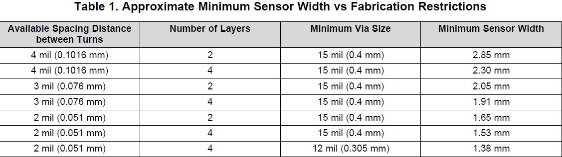
6. If we design a 3mm width sensor, is the sensor pocket (air gap) 0.3mm?

7. What is the inductance (uH) at a distance of 3mm?

  • Hi Alex,

    1. Can you clarify where the glass would be? Unless you are using an FR4 sensor coil, we do recommend adding stiffener to the back of the FPC.

    2. We recommend keeping the sensor as close as possible to the LDC. There is no minimum distance.

    3. We recommend using COM to shield INn above and below the trace. Note that COM is not GND. The LDC2114 will bias COM to ~0.9V. COM is the return path for the LC tank sensor.

    4. In general, the detection distance for an LDC device is 50% of the shortest side of the coil. In this case, the shortest side is 3mm, so the sensing distance is 1.5mm. However, for button replacement applications we recommend placing the target 0.1-0.2mm from the coil. 

    5. The button triggering condition is when the metal object moves closer to the sensor, which causes the sensor inductance and therefore the sensor frequency to shift. The material must be metal, and highly conductive metals like copper or aluminum are best. Note that copper or aluminum foil can be added to non-conductive materials. The target must move in order for the device to detect a button press.

    6. The air gap could be at most 0.3mm, but 0.1-0.2mm would be better.

    7. This depends on many variables, including your target properties and the design of your sensor. That graph is meant to be one example, but not a definitive guideline for every sensor.

    Best Regards,

  • Hi Kristin 

    Thanks for your reply, I have some questions are confused and need your help, thank you.

    1.Sorry for the misunderstanding. I mean the button material is glass, but like you said the non-conductive material needs to cooper or aluminum under the button, so we need to strain relief(red circle) on FPC too?

    2.can placement any component or signal trace under the sensor? How far is the recommended distance to the component?

    3. Could you please recommend INn trace width? INn both sides need to GND covering it?

    4. What is the minimum requirement inductance value and coil width of circular? if the sensor air gap is 0.2mm.

    5.If I use 2 layers of FPC, should I put silver paste on the TOP surface to meet COM INn COM rule?(like Q2 pic)

    6. Select coil geometry and other parameters website tool, is the layer means coil or INn?

  • Hi Alex,

    I'd be happy to help you further with this when I return to office in early January.

    Best Regards,

  • Hi Kristin

    Thanks for your answer to another topic question.

    Could you also reply to this topic question? thanks.

  • Hi Alex,

    I've answered your questions below:

    1. Yes, regardless of the housing material, the strain relief is a good idea.

    2. No, you should have a keepout area on all layers above and below your sensor. This includes power planes. The keepout area should extend beyond the outer edge of the coil by about 20% of the coil's diameter. We have additional layout guidelines in the LDC2114 datasheet.

    3. The INn traces should be at least 6 mil (0.15mm). This is discussed in section 10 of the datasheet. We recommend shielding both sides with COM, not GND. COM will be driven to ~Vdd/2 by the LDC2114. It is the return path for the sensor, which is then connected to GND through Ccom.

    4. There is no minimum inductance; however, there are a minimum sensor frequency (1MHz) and a minimum sensor Rp value (250 ohms). I suggest first designing your coil to fit your physical parameters, then seeing if you need to change the design at all to meet these requirements. I recommend using the Spiral Inductor Designer in the LDC Tools Excel Calculator (you can find this tool in the FAQ linked in my signature below).

    5. You could do this, but it is not necessary.

    6. The number of layers is for the coil. Realistically, they are the same, because the INn trace forms the coil.

    Best Regards,

  • Hi Kristin

    Thanks for your information, please help feedback as below questions. thanks.

    1.Can I cancel the strain relief and what are the side effects?  If we have space limitations.

    2. OK. The coils on the upper and lower layers will not place any components and traces.

    But this is the daughter board if the watch has a mainboard in the center.

    What is the minimum safety distance(mm) from the inside component or PCB when the coil install on the side?

    5. Is it possible to have two FPC layers? Only Inn and COM? I thought the minimum FPC layers are 3?

  • Hello Alex,

    My apologies for the delayed reply to this follow-up question. 

    1. If you remove the strain relief, there may be mechanical challenges associated with bending the FPC sensor. There may be too much strain on the sensor or on the FPC's connectors to the main board, which could cause long term mechanical reliability issues.

    2. I recommend separating the sensor from other components by at least the width of the short side of the sensor.

    5. We do recommend shielding both sides of the INn signal with COM, so you would need 3 signal layers for the FPC. The coil would only be present on two layers.

    Best Regards,