Hi,
I have some, probably basic, questions about complex-baseband architecture and request your kind guidance. The questions refer to TI document spyy007.pdf
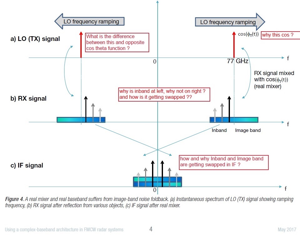
1- Please refer following fig on page 4 of above document, I have put the questions in figure also and I will repeat them in writing also after figure:
1a) What is the difference between right and left half of figure ?
1b) Refer part a LO(TX) signal. What is the difference between the red peak showing LO(TX) signal and the red peak with cos theta function ?
1c) Refer part b (RX signal). Why is Inband on left side and not on right side in the part of figure shown? How is getting swapped when seen and compared with cos theta red peak above it in part a ?
1d) Refer part c (IF). How are the Inbnad and Image Band getting swapped ?
1e) Can you please refer additional general and / or TI documents that explain more about complex-baseband architecture and interference mitigation achieved from the same ?
2- Refer page 8. It states: " In fact, it is possible to frequency-shift the spectrum, perform image-reject filtering and send out decimated I and Q ADC samples to the DSP at fb,max " and " TI’s radar chip includes a built-in digital frequency shifter to frequency-shift the samples, perform image-reject filtering and send out the complex baseband output at the reduced interface rate (similar to a real-only implementation). "
Please advise how are these above features implemented in the following:
by using DemoVisualizer (CLI command)
by using mmwave Studio (preferably version 2.0.0.2)
Thank you and regards


