This thread has been locked.

If you have a related question, please click the "Ask a related question" button in the top right corner. The newly created question will be automatically linked to this question.

IWR6843ISK-ODS: 50 Ohm microstrip and coplanar waveguide antenna trace width

Part Number: IWR6843ISK-ODS
Other Parts Discussed in Thread: IWR6843

The IWR6843ISK-ODS mmWave EVM PCB design specifies the following 50 Ohm antenna trace width/space:

  1. Microstrip: 12 mil width.
  2. CPW guide: 11.625 mils width and 9 mils spacing.  

Do these trace width and spacing have to be exact as in the reference design if we are to use RO3003 RF core material? The PCB board house we are working with came back with different trace widths in order to achieve 50 Ohms (see modeled line widths shown in red below). 

It is critical to have matching 50 Ohms traces, however are the antenna microstrip and CPW guide trace widths not as critical as long as 50 Ohms is achieved?

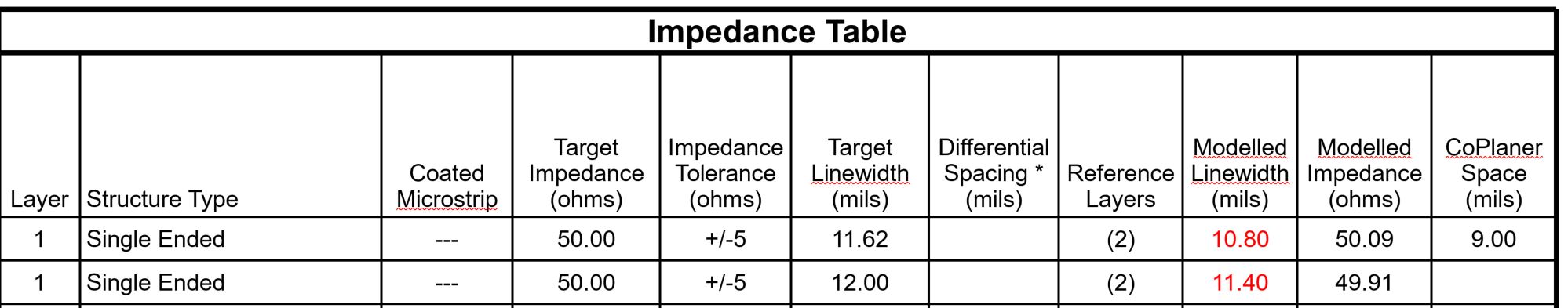
The new trace widths proposed by the board house to meet 50 Ohms are:

  1. Microstrip: 11.40 mils
  2. CPW guide: 10.80 mils


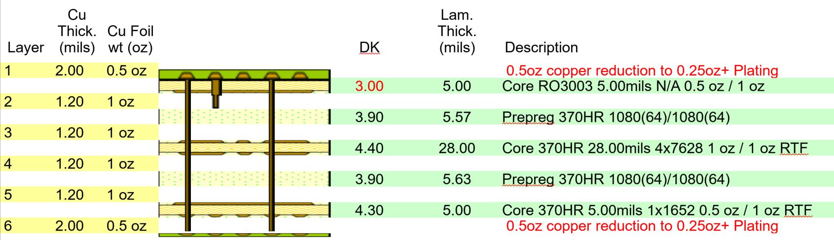
Proposed PCB stack-up

Thank you for all the help.

Christian.

  • Hi,

    The 50 ohms impedance is more critical. 

    please see linked appnote for manufacturing need-to-know.

    http://www.ti.com/lit/an/spracg5/spracg5.pdf

    BR,

    Charles O

  • Hi Charles,

    Thank you for the feedback. Yes,I had an opportunity to review this document.

    Basically, you are saying we can deviate from the IWR6843ISK-ODS trace widths to achieve the 50 Ohm impedance. 

    I was under the impression that if we are using the same RO3003 RF core, the antenna trace width should match exactly that of the EVM. Do you have information on what PCB impedance calculator TI used?

    Assuming we do use different microstrip and CPW trace widths than that of the EVM, Will this affect the geometry of the rectangular planar antenna portion?

    Regards,

    Christian.

  • Hi,

    If you are using the same material and the same stack up between RF layer and reference ground you should be able to copy the EVM and get the 50 ohms impedance. If its different then you need to ensure you have the right impedance.

    Br,

    Charles O 

  • Hi Charles,

    Thank you very much for confirming the antenna trace width question. This means the thickness of the 370HR prepreg material thickness is not critical, only the RF material core thickness.

    We are getting ready for prototype fabrication and have a couple of critical questions:

    1. Any concern with +/-1.5 mil solder mask tolerance / mis-registarion?
    2. Is antenna feature etching of +/-0.5 mils (within +/-0.7 max) acceptable?
    3. For drill size <= 12.2 mils, any concern with +2/-5.9 mil drill tolerance instead of +0/-5.9 size?
    4. Any concern if all 5.9 mil laser drills (including ones antenna ground area) are filled with non-conductive epoxy and plated?
    5. Is there impact to 50 Ohm RF impedance if the top layer antenna feature plating thickness is controlled to 1 mil +/- 0.2 as target and not exceed 1.4 mils? The fab house is proposing to start with 0.5oz RC RO3003 on top layer, reduce it down to 0.25 mils and then plated up to 1 mil +/- 0. 2 mils. The TI ODS stack-up shows the top layer thickness to be 0.8 mil after plating (is this correct?) Any concern about 1 mil top layer thickness versus the 0.8 mil in the ODS stack-up? Meaning do we need to recalculate RF trace widths?
    6. Is there impact to 50 Ohm RF impedance if we use 0.5oz/0.5oz RO3003 core versus 0.5oz/1oz RO3003 used in the ODS design. Meaning do we need to recalculate RF trace widths?

    Looking forward to your response.

    Regards,

    Christian.

  • Hello Christian,

        It is not advisable to change the RF traces width with as per 2D or 2.5D planer tools recommendation by the fab houses. Traces widths has been selected based on 3D EM field solver and appropriately de-rating the dielectric constant at desired frequency of operation. Hence recommendation is to stick to the dimensions detailed in the design.

    For other questions Please find the comments for your question below:

    1. Any concern with +/-1.5 mil solder mask tolerance / mis-registarion?

    [TI]  On the Antenna and RF traces solder mask is not applied, except at very short location on the RF balls to facilitate the soldering process. In other areas this tolerance is acceptable.

    2. Is antenna feature etching of +/-0.5 mils (within +/-0.7 max) acceptable?

    [TI] Yes, this is acceptable.

    3.For drill size <= 12.2 mils, any concern with +2/-5.9 mil drill tolerance instead of +0/-5.9 size?

    [TI] This tolerance is very high for laser drills, This may cause problem for the RF traces/Antenna and BGA to PCB transition regions. Could you revisit with FAB house on this spec.

    4. Any concern if all 5.9 mil laser drills (including ones antenna ground area) are filled with non-conductive epoxy and plated?

    [TI] Yes, it could be filled with non-conductive epoxy and plated. Plating thickness need to be controlled.

    5.Is there impact to 50 Ohm RF impedance if the top layer antenna feature plating thickness is controlled to 1 mil +/- 0.2 as target and not exceed 1.4 mils? The fab house is proposing to start with 0.5oz RC RO3003 on top layer, reduce it down to 0.25 mils and then plated up to 1 mil +/- 0. 2 mils. The TI ODS stack-up shows the top layer thickness to be 0.8 mil after plating (is this correct?) Any concern about 1 mil top layer thickness versus the 0.8 mil in the ODS stack-up? Meaning do we need to recalculate RF trace widths?

    [TI]    As plating thickness is not well controlled uniformly across the Antenna and RF regions, this causes non-uniformity on the thickness this could adversely affects the matching of RF traces (S11 parameter), Hence its not recommended to reduce it & re-plate it.

             6.Is there impact to 50 Ohm RF impedance if we use 0.5oz/0.5oz RO3003 core versus 0.5oz/1oz RO3003 used in the ODS design. Meaning do we need to recalculate RF trace widths?

    [TI] 0.5oz/1oz RO3003 Core would be better choice, Layer 2 is ground, as it improves the conductivity with the thicker cu. Also it helps in better thermal conductivity across the board. 

    Thanks and regards,

    CHETHAN KUMAR Y.B. 

  • Hi Chethan,

    Thank you for the detailed response.

    1. Is there a PDF that shows the critical dimensions of the IWR6843 ODS mmWave module's antenna structure?

    2. For top and bottom copper layer thickness is the following understanding correct? 0.5oz copper + immersion silver plating = 0.8mils total thickness. What is the maximum allowed plating tolerance?

    regards,

    Christian.

  • Hi,

    Can you extract this dimensions from the altium database provided online?

    BR,

    Charles O