


Other Parts Discussed in Thread: AWR1843
Tool/software: Code Composer Studio
Hi,
In the mmwave_sdk_03_03_00_03,for the AWR1843, the file c674x_linker.cmd is as follows:
#define L1P_CACHE_SIZE (16*1024)
#define L1D_CACHE_SIZE (16*1024)
#define MMWAVE_L3RAM_SIZE (MMWAVE_L3RAM_NUM_BANK*MMWAVE_SHMEM_BANK_SIZE)
MEMORY
{
PAGE 0:
#if (L1P_CACHE_SIZE < 0x8000)
L1PSRAM: o = 0x00E00000, l = (0x00008000 - L1P_CACHE_SIZE)
#endif
#if (L1D_CACHE_SIZE < 0x8000)
L1DSRAM: o = 0x00F00000, l = (0x00008000 - L1D_CACHE_SIZE)
#endif
L2SRAM_UMAP1: o = 0x007E0000, l = 0x00020000
L2SRAM_UMAP0: o = 0x00800000, l = 0x00020000
L3SRAM: o = 0x20000000, l = MMWAVE_L3RAM_SIZE
HWA_RAM : o = 0x21030000, l = 0x00010000
HSRAM: o = 0x21080000, l = 0x8000
/* PAGEs 1 and onwards are for overlay purposes for memory optimization.
Some examples:
1. Overlay one-time only text with uninitialized data.
2. Overlay L1PSRAM data path processing fast code and use copy tables
to page in (before entering data path) and out of L1PSRAM (when entering
sleep/low power).
*/
PAGE 1:
L3SRAM: o = 0x20000000, l = MMWAVE_L3RAM_SIZE
}
....
The first question is that what is the difference between the Page 0 and Page1?
The second one is the start address and length for the L3SRAM is identical, why?
The finall one is in the docment ,the L3SRAM is as belows:
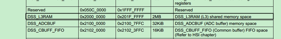
why is the address for L3SRAM on the Page 0 and Page 1 0x20000000? In the map file, how to distinguish them?
Thanks,
Regards,
Rata
