This thread has been locked.

If you have a related question, please click the "Ask a related question" button in the top right corner. The newly created question will be automatically linked to this question.

IWR6843ISK: Questions about IWR6843ISK PCB?

Part Number: IWR6843ISK
Other Parts Discussed in Thread: IWR6843

hi. this is jiyoung 

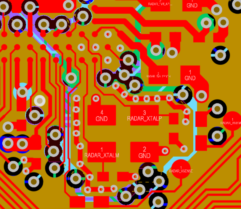
and currently i'm making RADAR PCB using IWR6843.

see the reference model which is given by TI.

i have some questions.

from the reference design,

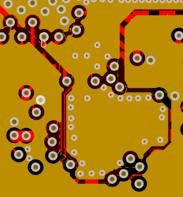
the microvias connect 1-2 in the RF part

and there are additional vias to connect L1-L4-L6, but there are just a few and the number of them is 7

i think it's because there are some components are located at the bottom side of PCB.

if there aren't any component and there are many empty spaces, is it better to have 1-8 additional vias as many as possible? 

this is my first questions

and my second questions is

from the reference design, second layer is separated into two GND planes.

i think the reason why doing this is be cautious about PWR, DIGITAL noise which can disturb the RF signals 

but what about the crystal noise? crystal and RF grounds are connected from the reference design.

is the crystal noise is so higher(25MHz) than IF frequencies so do you think it is unnecessary to consider the noise from crystal? 

if there are any considerations or explanations about designing RF PCBs, 

please let me know.

i already have a "HardwareDesignCheckList_Vp08_IWR6843"

look forward your reply

thank you:)

  • Hello Jiyoung,

     For the first question,  You are right, it there are more spaces we could add more vias and distribute more evenly as needed. 

    There are two vias types that are most important 1) Layer 1 to 2 : This is mainly for RF lines which connect to 2nd Layer ground 2) Plated Through vias which connects respective layer depending upon routing requirements. Depending upon space available plated through vias could be deployed. However too many PTH vias (Mainly due to Anti-pad rules of via) also perforates planes and makes ground and power integrity weaker. Hence care need to be taken to provide optimally. 

    Second question: Very good question!. 

    We do add via fence around the crystal (not ideal though!), as shown below in the layout image.

    And in the 2nd Layer a cut out is done as shown below.   

    Crystal circuit refereed to RF ground.  Crystal is not an aggressor, rather it's victim of other signals coupling to crystal pins, Crystal pins CLKP and CLKM are high impedance nodes, which are susceptible for aggressor in the design (Such as PMIC switching nodes, LVDS clocks etc). Hence it's need to shielded, However care need to be taken during  the shielding not to add additional parasitic which will disturb the crystal intentional capacitors. 

    Thanks and regards,

    CHETHAN KUMAR Y.B.