This thread has been locked.
If you have a related question, please click the "Ask a related question" button in the top right corner. The newly created question will be automatically linked to this question.
Dear support team.
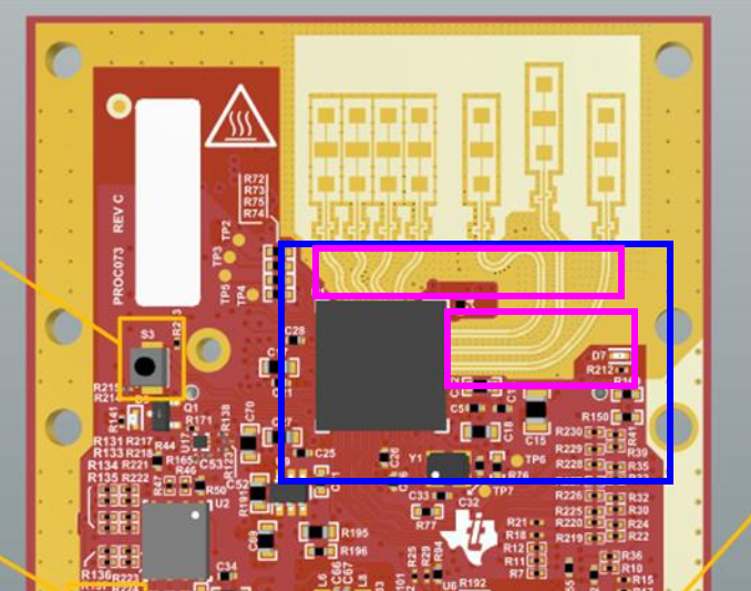
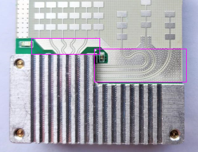
I am kicking off a new design based on IWR6843, currently I used the IWR6843ISK-ODS as a design reference. because of our application environment, I want to stuff a heatsink on the top side of IWR6843, and it will cover the whole area show in the below blue block. Could you help confirm whether the RF traces in the pink block are the effective antenna areas? I want to know if these areas can be covered by a matellic heatsink ? Is it necessary for me to design a heatsink like below example, which exposed the whole RF traces area, but the area of heatsink is limited.
Regards.
Hello,
Thank you for sharing your experience. Above diagram is for IWR6843ISK reference design.
It's preferable to avoid the RF lines for the metallic heat sink, As it might disturb the impedance of the grounded co-planar wave guide traces.
If it's absolutely needed then around the RF traces height of the metallic structure should be more than 2mm above the RF traces to avoid EM field coupling to the metallic heat-sink surface.
Also care need to be taken heat-sink should not come close to Antenna region. On the above blue box top side of the blue box is very close to antenna matching elements, at least better to retract it at-least by 2mm.
Thanks and regards,
CHETHAN KUMAR Y.B.