This thread has been locked.

If you have a related question, please click the "Ask a related question" button in the top right corner. The newly created question will be automatically linked to this question.

CCS/PGA900: PGA900 DAC

Part Number: PGA900

Tool/software: Code Composer Studio

Hello ;

section 1:

Voltage measured between GND pin in the PGA900 and negative terminal of
the controller. This includes the internal 40-Ω resistor and an external 10-Ω
resistor, VDD = 15 V. The DAC codes used were 0x880 and 0x2760 for 4 and
20 mA respectively.(PGA900 datasheet SLDS258  Page )
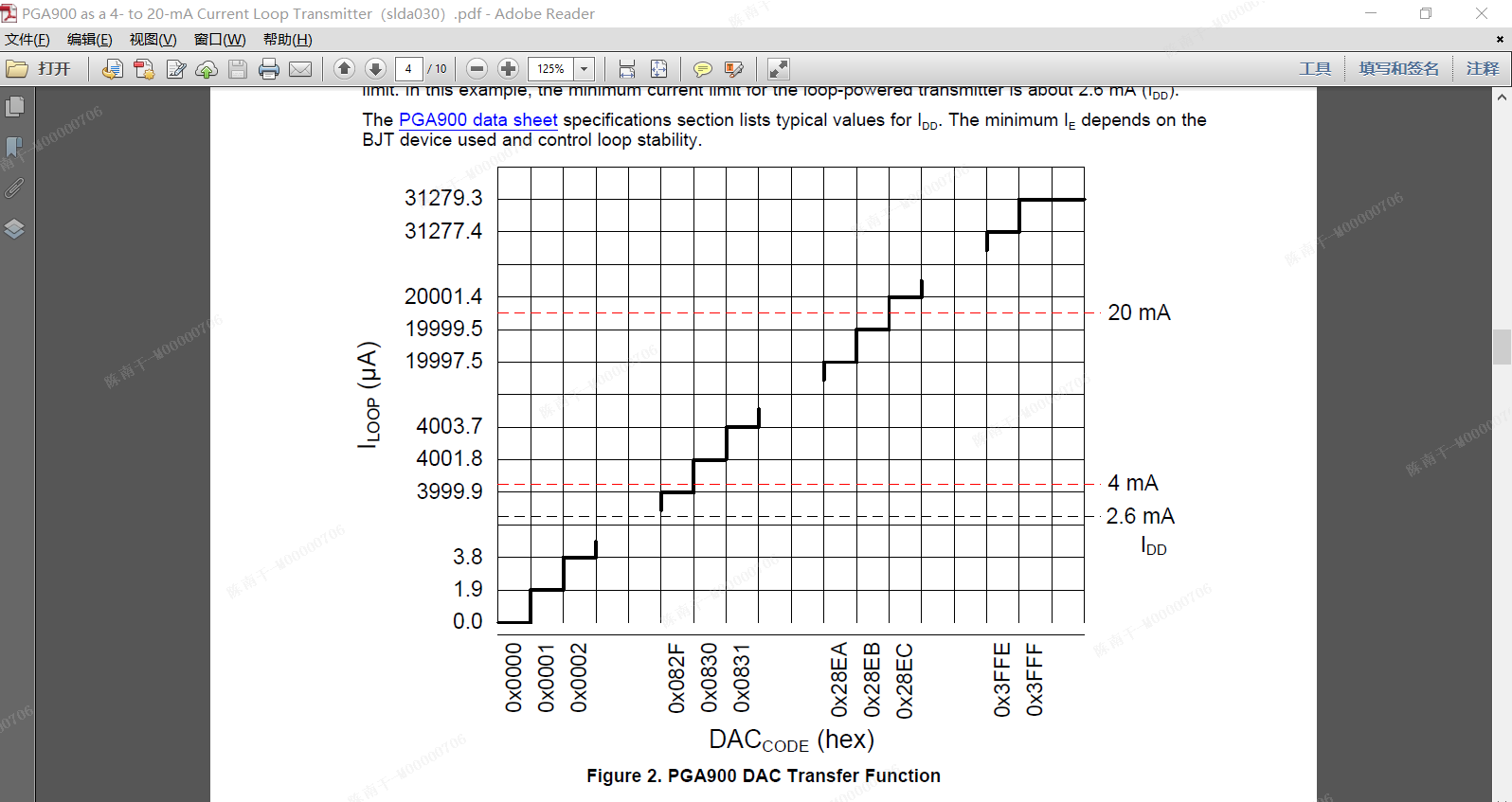
section 2:
 The DAC codes used were 0x830 and 0x28EB for 4 and
20 mA respectively.(PGA900 as 4 to 20 mA C urrent loop Transmitter SLDA030)

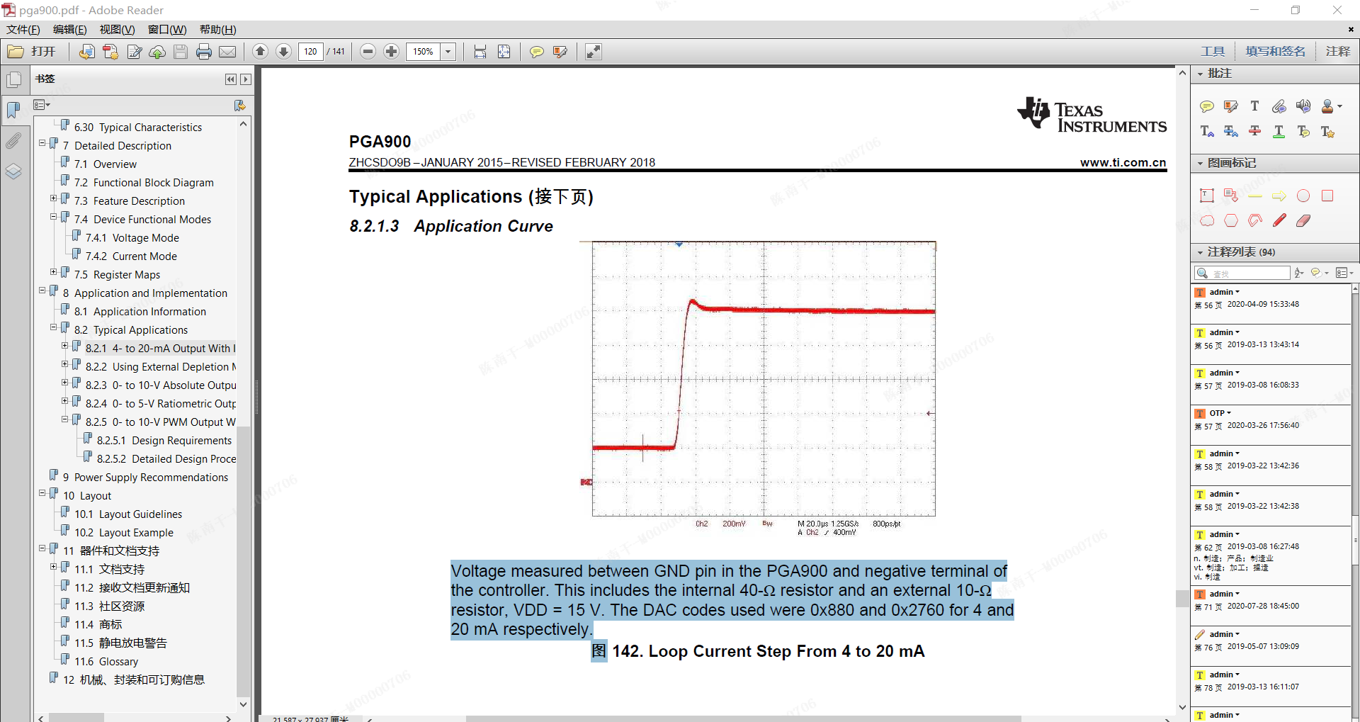
So what is more  correct?

  • Hello Chennangan,

    The plot from the "PGA900 as 4 to 20 mA Current loop Transmitter SLDA030" application note is a direct result of Equation 1 from that application note. It is an ideal graph that does not take into account DAC offset or gain error.

    The application curve from the datasheet shows real measured data from a specific PGA900 device. The offset and gain error of that particular device caused it to deviate somewhat from the ideal values described in the application note. The difference between the two values is within the 3.5% FSO error of the DAC in current operating mode. This error can be compensated for when doing the device calibration procedure.


    Regards,

  • Hello  Scott:

    I try different  PGA900 chips  on the same PGA900EVM . The same DAC_REG0  output   can  case different  current output  in current operating mode .

    Does It means that  I should  do all of devices  calibration procedure

  • Hello Chennangan,

    Yes, for the best accuracy and consistency among sensors you will need to perform a calibration for each one.


    Regards,