This thread has been locked.

If you have a related question, please click the "Ask a related question" button in the top right corner. The newly created question will be automatically linked to this question.

PGA411Q1EVM: PGA411 AFE Fault

Part Number: PGA411Q1EVM

Hello,

I'm trying to tweak the values of the AFE for the PGA411 and I'm running into some problems.

According to the datasheet the VIZx signals should be centered around 0.5*Vcc (2.5V) but in my case this is not true. They are centered around 1.9V. This is making things a little bit complicated because all of the high and low voltage thresholds for all of the fault diagnostics assumes this. I have checked the COMAFE pin and it is indeed 2.5V and I have also checked the OSIN and OCOS signals and they are also centered around 2.5V.

This is a screenshot of one of my VIZx (the rest look the same):

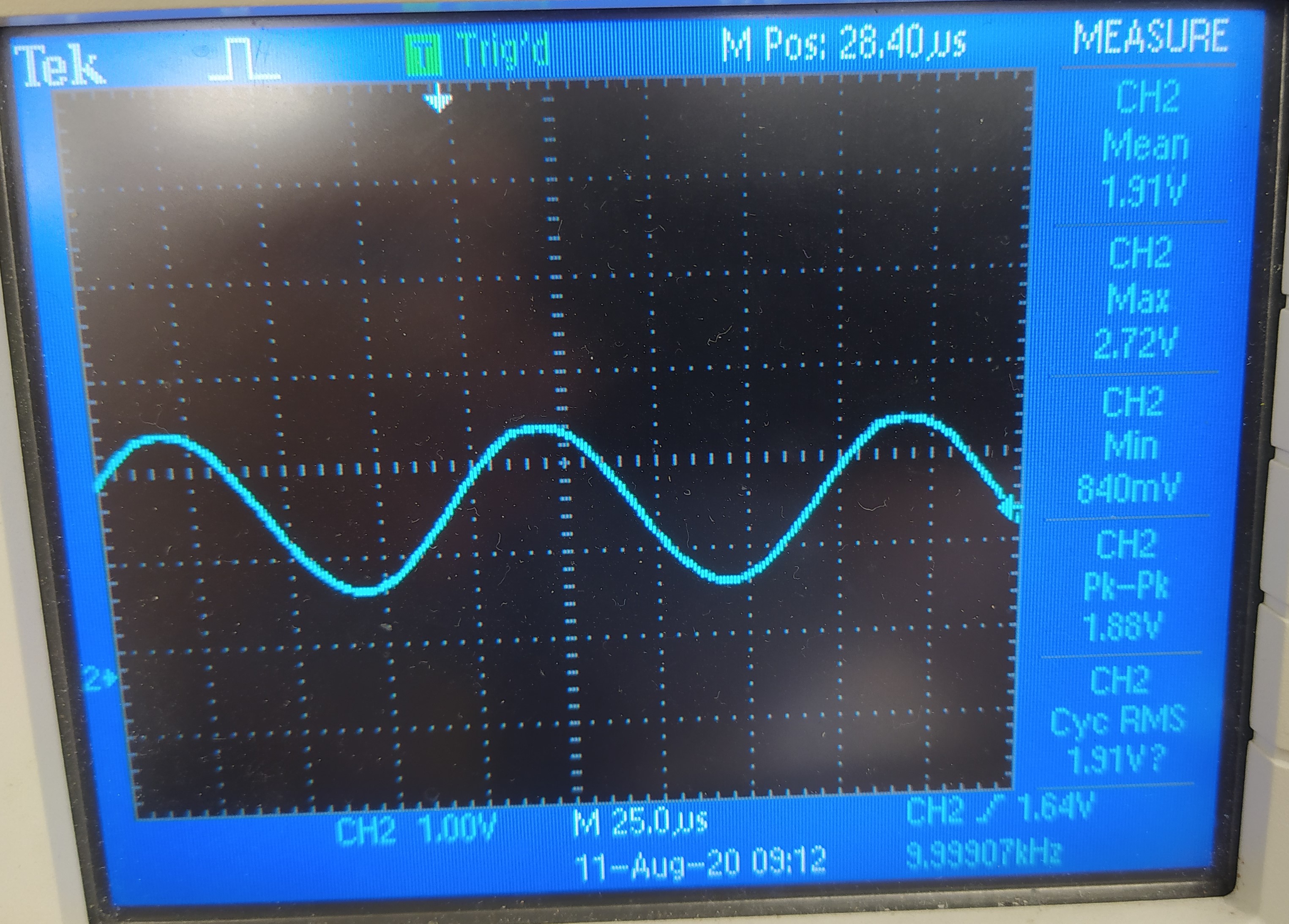
Any ideas why this is happening?

  • I have removed all of the pull-ups and pull-down resistors (for the open circuit detection) and the average voltage has gone up quite a bit to 2.23V, Not quite yet 2.5V but much closer. I have been using the EVM. Is it possible that those resistors are too small and bias the VIZx signals excessively?

  • I have a few more questions:

    - The datasheet recommends the IZx to be a maximum of 3Vpp. However the maximum and minimum thresholds for the OMIZ faults is 1.35V and 3.65V which means that any signal (assuming it is perfectly centered around 2.5V which is not my case) bigger than 2.3V will be detected as an integrity fault isn't? Should the IZx signals be limited then to a maximum of 2.3Vpp (or even less if they are not perfectly centered)?

    - In the datasheet, page 88, the example says that the OSIN and OCOS output swing should always be less than 4Vpp, but the IZx have to be 2Vpp to avoid triggering the integrity check fault. Does this mean that the SIN/COS signals (as they come out of the resolver) have to be scaled down to 2Vpp and scaled back up using the internal amplifier to 4Vpp? This sounds like a really bad idea since the signal to noise ratio would be greatly reduced, isn't?

    - What is the recommended value to use for the VEXT voltage generated by the exicter power supply? I need to supply a 7Vrms resolver, but I think I can do this with the VEXT voltage set to 13-17V. Any reason to pick one value or another?

    - Another thing I have noticed is that I was expecting the IZ2/IZ4 and IZ1/IZ3 to have a very similar waveform in terms of amplitude (at its maximum and minimum point, 180 degrees off). However I have noticed that they are not. In particular with my current settings I can see in IZ4 a maximum of 1.36Vpp and in IZ2 I can measure a maximum of 1.9Vpp. This is a very big difference, would you expect this? Is this due to an offset on the mechanical mounting of the resolver?

    - The ORS pin output seems to be a fixed 1.7V despite the fact the VOE pins look like they should and give me a good excitation signal. I was expecting this pin to output the preamplifier exciter signal.

  • Hi Javier,

    Please find my responses below.

    1&2. 

    Please use the same values, let's say 50k each for both pullup and pull down. This will make the common mode to be 2.5V.

    For best performance, the amplitude of OSIN and OCOS should be between 600mVpp to 1.5Vpp. So, we need to adjust all other values to meet this requirement. The fault thresholds should be adjusted around these values.

    Below is the recommendation from datasheet-

    "The AFE block connects to the SIN and COS coils of the resolver sensor where the SIN (IZ2
    and IZ4) and the COS (IZ1 and IZ3) signals are amplified by differential input amplifiers with variable gain. The
    amount of gain is determined independently by the SINGAIN and COSGAIN bits in the DEV_AFE_CFG register.
    The selected gain can be between 0.75 to 3.5. For best accuracy performance, TI recommends that the IZx
    differential voltage (VPP) is between 600 mVPP and 1.5 VPP as measured at the OSIN and OCOS pins. The gain
    settings GAINSIN and GAINCOS SPI settings can be adjusted to optimize this signal. For example if the input to
    the IZx pins is between 800 mVPP and 2 VPP, setting GAINSIN = GAINCOS = .75 gain would give you the
    optimum VPP of between 600 mVPP and 1.5 VPP on the OSIN and OCOS pins. The single ended voltage
    requirements on the IEx and IZx pins is between 0.5 V to 4.5 V"


    Additionally, please refer to AFE Design Guide and Fault Diagnostics for further information

    3. Please chose EXTOUT_GL the EXTOUT to adjust the gain and VCOM for the desired peak to peak and common mode exciter signal. Based on this, please chose VEXT so that the min value is at least 1V higher than the exciter output signal(Figure 14).

    4. Yes, it is related to Resolver configuration. Generally, this should not cause any issues if the OSIN and OCOS amplitudes are the same.

    5. The ORS output of the exciter preamplifier is controlled by the XEXT_AMP bit in the DEV_OVUV2 register. When this bit is set to 1, external amplifier mode is selected which enables the ORS output and disables the internal output-power amplifier. However, the default state of this bit is 0 which means that the ORS output is disabled and the internal output-power amplifier is enabled.

    Regards

    Sharath.

  • Thank you very much for the prompt support. It was very useful.

    I didn't know that AFE Design Guide existed at all.

    I just wanted to point out a little bit of a contradiction (or maybe misunderstanding) that I have found. In the AFE Design Guide the pull-up pull-down resistors are recommended to be set to 15/25kOhm depending on the mode but in the datasheet they recommend (page 89) different values. I have had quite success with using both 15kOhm as recommended in the AFE Design Guide (I'm using 7Vrms mode), however with the datasheet recommendations (table 45) I end up with strange DC offsets on the IZx pins (according to that table I should be using 50kOhm and 20kOhm). I believe instead of being a function of the VEXT voltage, shouldn't it be a function of the QVcc voltage? 

  • Hi Javier,

    Yes, I agree with you. Different values were used in different places to solve certain fault detection conditions. 

    VEXT voltage provides DC bias to the IZx pins. It is a combination of QVCC pull up&pull down resistors, and the VEXT voltage determines the voltage on IZx pin when a Coil open condition is present. This IZx voltage will be compared against OPENTH to detect an open fault. I recommend testing for open conditions and decide whether the resistors you chose will work or not.

    Regards

    Sharath.

  • Thanks very much for your help. =)

    We can close the issue.