This thread has been locked.

If you have a related question, please click the "Ask a related question" button in the top right corner. The newly created question will be automatically linked to this question.

PGA970: PGA970 EVM Diagnostics Issues

Part Number: PGA970

Hi,

I'm developing on a PGA970EVM and can't get the DAC to Output the Voltage, because the FaultDiag value is always set to one which disables writing the value to the output register.

When watching the Memory Registers in the debugger, I instantly get several Diagnostics Errors right after reset:

PSMON1    00000000b (Binary)  PSMON1 Fault Detect Register [Memory Mapped]
PSMON2    00010000b (Binary)  PSMON2 Fault Detect Register [Memory Mapped]
AFEDIAG   00000000b (Binary)  AFEDIAG Register [Memory Mapped]
AFEDIAG1 00110011b (Binary)  AFEDIAG1 Register [Memory Mapped]
AFEDIAG3 00110011b (Binary)  AFEDIAG3 Register [Memory Mapped]
AFEDIAG4 00110000b (Binary)  AFEDIAG4 Register [Memory Mapped]

I always get the exact same Diagnostics Errors.

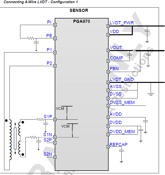
The only things plugged into my EVM are a 12V PSU and a LVDT in 4 Wire Connection like this:

Any Ideas what could cause this or how to resolve this issue?

  • Hi Remo,

    During the initial setup of the PGA970 in your firmware do you clear all of the faults? Writing 1 to each of the available AFEDIAGx and PSMONx bits will clear them, and then any faults detected later will be latched to the registers.

    Can you post the contents of the AFEDIAG_CFG register?


    Regards,

  • AFEDIAG_CFG is always 0x00.

    The registers are cleared in APP_Reset_Init() like this:

    FaultDiag = 0;

    PSMON1 = 0xFF;

    PSMON2 = 0x1F;

    AFEDIAG = 0xFF;

    AFEDIAG1 = 0xFF;

    AFEDIAG3 = 0xFF;

    AFEDIAG4 = 0xFF;

    The Afediag register seem to ignore this reset compleatly. When I step through the program, nothing happens when I get to those lines. Also when writing 0x5F, to PSMON2 to enable the Oscillator-good check, I get this message repeatedly in the console:

    Cortex_M0_0: Error: (Error -615 @ 0x0) The target failed to see a correctly formatted SWD header. The connection to the target may be unreliable. Try lowering the TCLK setting before trying again. (Emulation package 6.0.407.3)
    Cortex_M0_0: Trouble Halting Target CPU: (Error -2064 @ 0x0) Unable to read device status. Reset the device, and retry the operation. If error persists, confirm configuration, power-cycle the board, and/or try more reliable JTAG settings (e.g. lower TCLK). (Emulation package 6.0.407.3)

    I am really at a loss here, because the registers simply don't respond to things I am doing.

  • I may have stumbled upon a serious mistake in the reference firmware:

    in pga970_diag.h, the AFEDIAG_CFG Bit definition is as Follows:

    #define S1_PULL_UP_ENABLE (0 << 0)
    #define S1_PULL_UP_DISABLE (1 << 0)
    
    #define S2_PULL_UP_ENABLE (0 << 1)
    #define S2_PULL_UP_DISABLE (1 << 1)
    
    #define S3_PULL_UP_ENABLE (0 << 2)
    #define S3_PULL_UP_DISABLE (1 << 2)
    
    #define PE_PULL_UP_ENABLE (0 << 3)
    #define PE_PULL_UP_DISABLE (1 << 3)

    where as in the datasheet register map it is defined as:

    0

    0: Disables pullup used for open/short diagnostics on S1 pins
    1: Enables pullup used for open/short diagnostics on S1 pins

    1

    0: Disables pullup used for open/short diagnostics on S2 pins
    1: Enables pullup used for open/short diagnostics on S2 pins

    2

    0: Enables pullup used for open/short diagnostics on AIN1 pin
    1: Disables pullup used for open/short diagnostics on AIN1 pin

    3

    0: Disables pullup used for open/short diagnostics on PE pins
    1: Enables pullup used for open/short diagnostics on PE pins

    4:7 Reserved

    where it seems inverted for 0, 1 and 3 and only correct for bit 2.

    is there a reason for the difference, I am not seeing?

  • Hi Scott, 

    do you have any updates on the topic?

    Regards

  • Hi Remo,

    I've noticed that there's a discrepancy in the datasheet between the register map section and the technical description section in how it is described that you should clear the diagnostic faults. In the technical description section it says that they are cleared by writing a logic 0, while the register map shows it is cleared with a logic 1. If writing the logic 1 does not seem to clear them, then it is likely that they should be cleared with a logic 0 instead. I am confirming this with a designer.


    The debugger error only occurs when you set the PSMON2 register? Does it matter what you write to the register, or does it happen regardless of the data?

    I believe that the firmware is actually correct as far as the enabling and disabling of the pullups is concerned. I think that the datasheet is correct for bit 2, but incorrect for the others. I am confirming this along with the correct setting to clear the faults.

    Regards,