This thread has been locked.

If you have a related question, please click the "Ask a related question" button in the top right corner. The newly created question will be automatically linked to this question.

TDC7201: why TDC7201 don't response my read response?

Part Number: TDC7201
Other Parts Discussed in Thread: TDC7200, MSP430F5529

Dear ,

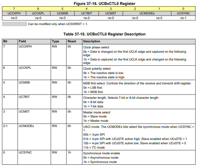
       I use SPI to communicate with TDC7201.

I use SPI Mode 0 CPOL=0, CPHA=0.

16M clock is checked OK. Enable pin is high.

But TDC don't response my read command.

Do you have any reference code ?

I send 0x80, or 0x81. 


  • user4523305,

    You can find reference code for the TDC720x in the "TDC720xEVM_Firmware_Source-v2.07.zip" of the install directory of the TDC720xEVM GUI Installer v2.1.8.0 (Rev. E) at "C:\Program Files (x86)\Texas Instruments\TDC720xEVM\Firmware". The "TDC7200_basic_spi_rw" CCS project is a good place to start.

  • Hi Akeem Whitehead,

             I checked the code ""TDC7200_basic_spi_rw"",

    But SPI initial is all registor setting.

    I can't understand which SPI mode and speed it set in function.

    attached for your reference. 

           Would you teach me which SPI mode and speed it use? 

    //------------------------------------------------------------------------------

    //------------------------------------------------------------------------------
    //  void TI_TDC720x_SPISetup(void)
    //
    //  DESCRIPTION:
    //  Configures the assigned interface to function as a SPI port and
    //  initializes it.
    //------------------------------------------------------------------------------
    void TI_TDC720x_SPISetup(void)
    {
      TI_TDC720x_CSB1_PxOUT |= TI_TDC720x_CSB1_PIN;
      TI_TDC720x_CSB1_PxDIR |= TI_TDC720x_CSB1_PIN;                                // /CS disable
      
      TI_TDC720x_CSB2_PxOUT |= TI_TDC720x_CSB2_PIN;
      TI_TDC720x_CSB2_PxDIR |= TI_TDC720x_CSB2_PIN;  

      UCB0CTL1 |= UCSWRST;                                                         // **Disable USCI state machine**
      UCB0CTL0 |= UCMST+UCMSB+UCCKPH+UCSYNC;                                       // 3-pin, 8-bit SPI master 
      UCB0CTL1 |= UCSSEL_2;                                                        // SMCLK
      //
      UCB0BR0 = 0x02;                                                              // UCLK/2 (should be 2MHz for 4MHz SMCLK)
      UCB0BR1 = 0;

      TI_TDC720x_SPI_USCIB0_PxSEL1 |= TI_TDC720x_SPI_USCIB0_SIMO
                                       | TI_TDC720x_SPI_USCIB0_SOMI;              
      TI_TDC720x_SPI_USCIB0_PxSEL2 |= TI_TDC720x_SPI_USCIB0_UCLK;
                                                                                   // SPI option select
      TI_TDC720x_SPI_USCIB0_PxDIR1 |= TI_TDC720x_SPI_USCIB0_SIMO;
      TI_TDC720x_SPI_USCIB0_PxDIR2 |= TI_TDC720x_SPI_USCIB0_UCLK;

                                                                                   // SPI TXD out direction
      
      UCB0CTL1 &= ~UCSWRST;                                                        // **Initialize USCI state machine**

      // Test reading DOUT1 and DOUT2 in parallel
      // initialize UCB1 as the second spi port  
      UCB1CTL1 |= UCSWRST;                                                         // **Disable USCI state machine**
      // make sure it is in slave mode
      UCB1CTL0 &= ~UCMST; 
      UCB1CTL0 |= UCMSB+UCCKPH+UCSYNC;                                             // 3-pin, 8-bit SPI slave 

      TI_TDC720x_SPI_USCIB1_PxSEL1 |= TI_TDC720x_SPI_USCIB1_SIMO
                                       | TI_TDC720x_SPI_USCIB1_SOMI;              
      TI_TDC720x_SPI_USCIB1_PxSEL2 |= TI_TDC720x_SPI_USCIB1_UCLK;
                                                                                   // SPI option select
      TI_TDC720x_SPI_USCIB1_PxDIR1 |= TI_TDC720x_SPI_USCIB1_SIMO;
      TI_TDC720x_SPI_USCIB1_PxDIR2 |= TI_TDC720x_SPI_USCIB1_UCLK;
                                                                                   // SPI TXD out direction
      
      UCB1CTL1 &= ~UCSWRST;                                                        // **Initialize USCI state machine**

    }
  • user4523305,

    According to the TDC7201's datasheet "Figure 1. SPI Register Access: 8 Bit Register Example", data is latched on rising edge of SCLK (CPHA=0) and the clock idles at 0 (CPOL=0). This combination is SPI MODE 0 as you first correctly indicated. 

    To better understand how the SPI is confgiured on the MSP430F5529, you'll need to refer to the MSP430x5xx and MSP430x6xx Family User's Guide (Rev. Q). This document explains the details of the UCB0CTLx registers of the TDC7200_basic_spi_rw example. For example, in the following line of code:

    UCB0CTL0 |= UCMST+UCMSB+UCCKPH+UCSYNC; // 3-pin, 8-bit SPI master

    The default value of '0' is used for UCCKPL for "inactive state is low", and UCCKPH is set to '1' for "data captured on the first UCLK edge and changed on the following edge". This effectively sets SPI MODE 0. See the following UCBxCTL snippet from the family user's guide for details: