1.
Our pcb fab said,galvanic effect at the junction between antenna and solder mask may affect antenna signal,if we insist on immersion silver,is galvanic a problem?
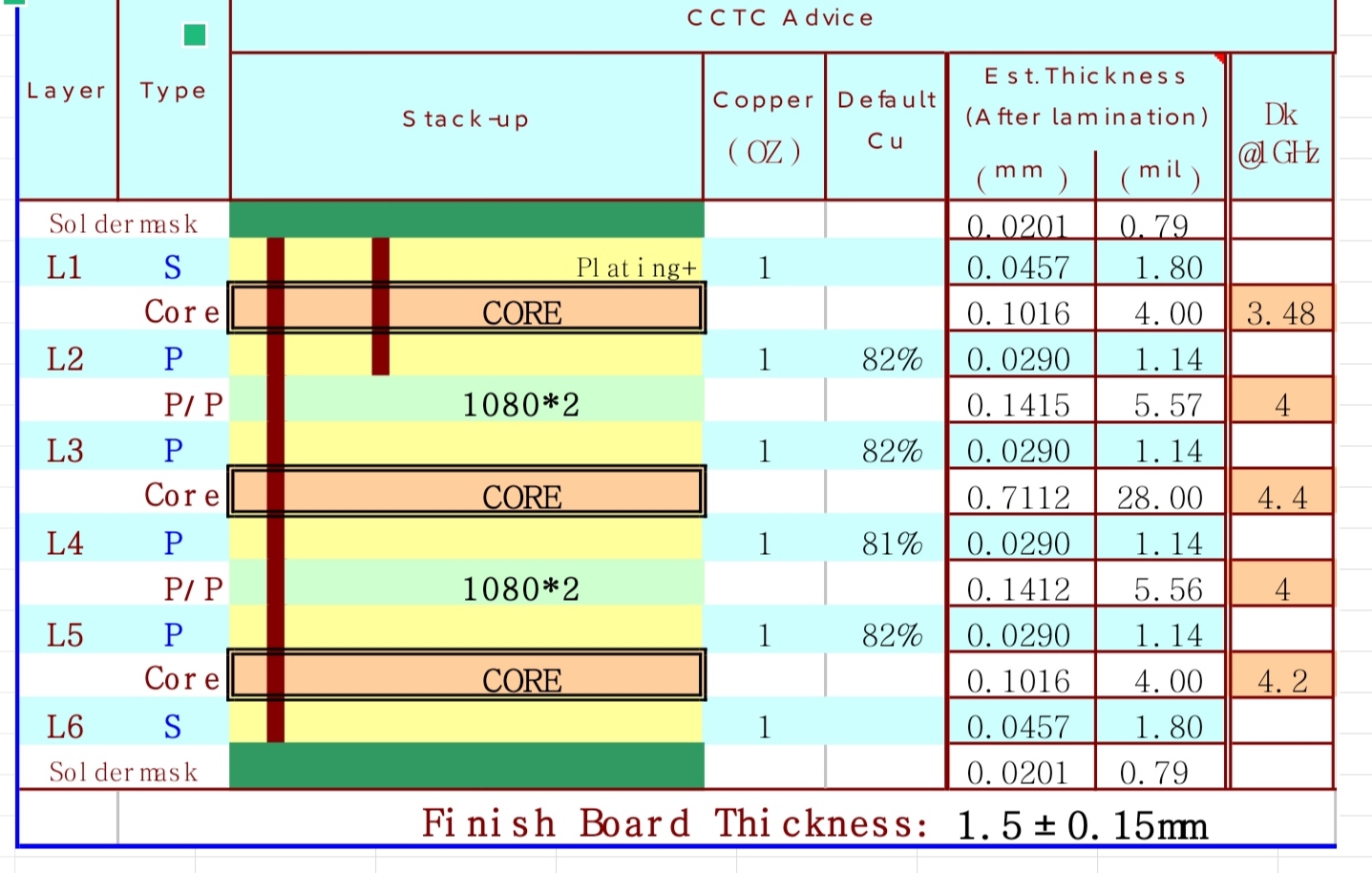
2.shengyi technology s1000
pcb fab recommended another stackup,L1-L2 is ro4835,L3-L6 is shengyi technology s1000(FR4).
we are not sure if this stackup and FR4material are avaliable.
And the thickness of layer copper is OK?
3.
In the PROC073B fabnotes,PTH copper thickness is 20um_30um.There is no thickness about L1-L2 blind hole copper thickness.what is requirement of the blind hole.
our pcb fab provide a design:PTH copper thickness average 25um,min 20um.
blind hole copper thickness average 18um,min 15um.is this design OK?
4.
What is the requirement of copper thickness and tolerance about antenna,
and what is requirement of antenna width tolerance?
our pcb fab said if antenna copper thickness 18um+/-5um;and another part is 45um+/-10um,but 8mil,10mil,12mil PTH can not be filled and solder.
Another solution is antenna and other part thickness is 45um+/-10um,8mil、10mil、12mil PTH can be filled,and tolerance of antenna width is 25um.
5
5.What is requirement of copper thickness of antenna,including base copper and finished copper?
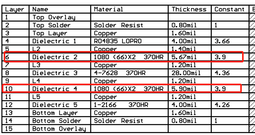
6.L1-L2 PCB material Rogers 4835 4mil core1/1 Low Pro is OK? what are differences of H/H、1/1、H/1.
our pcb fab can afford Rogers 4835 4mil core1/1 Low Pro and Rogers 4835 4mil coreH/H Low Pro.Which one is better choice?
7. our pcb fab said:whatever surface finish,L1-L2 blind via can not be filled? is this real? Will unfilled blind via affect antenna signal?
8.Our pcb fab said if 50ohm antenna traces can not match 50ohm,can they adjust antenna trace width?Or according to the original size, do not control impedance.
Thanks.