Because of the holidays, TI E2E™ design support forum responses will be delayed from Dec. 25 through Jan. 2. Thank you for your patience.

This thread has been locked.

If you have a related question, please click the "Ask a related question" button in the top right corner. The newly created question will be automatically linked to this question.

FDC2214: Communication interruption

Part Number: FDC2214

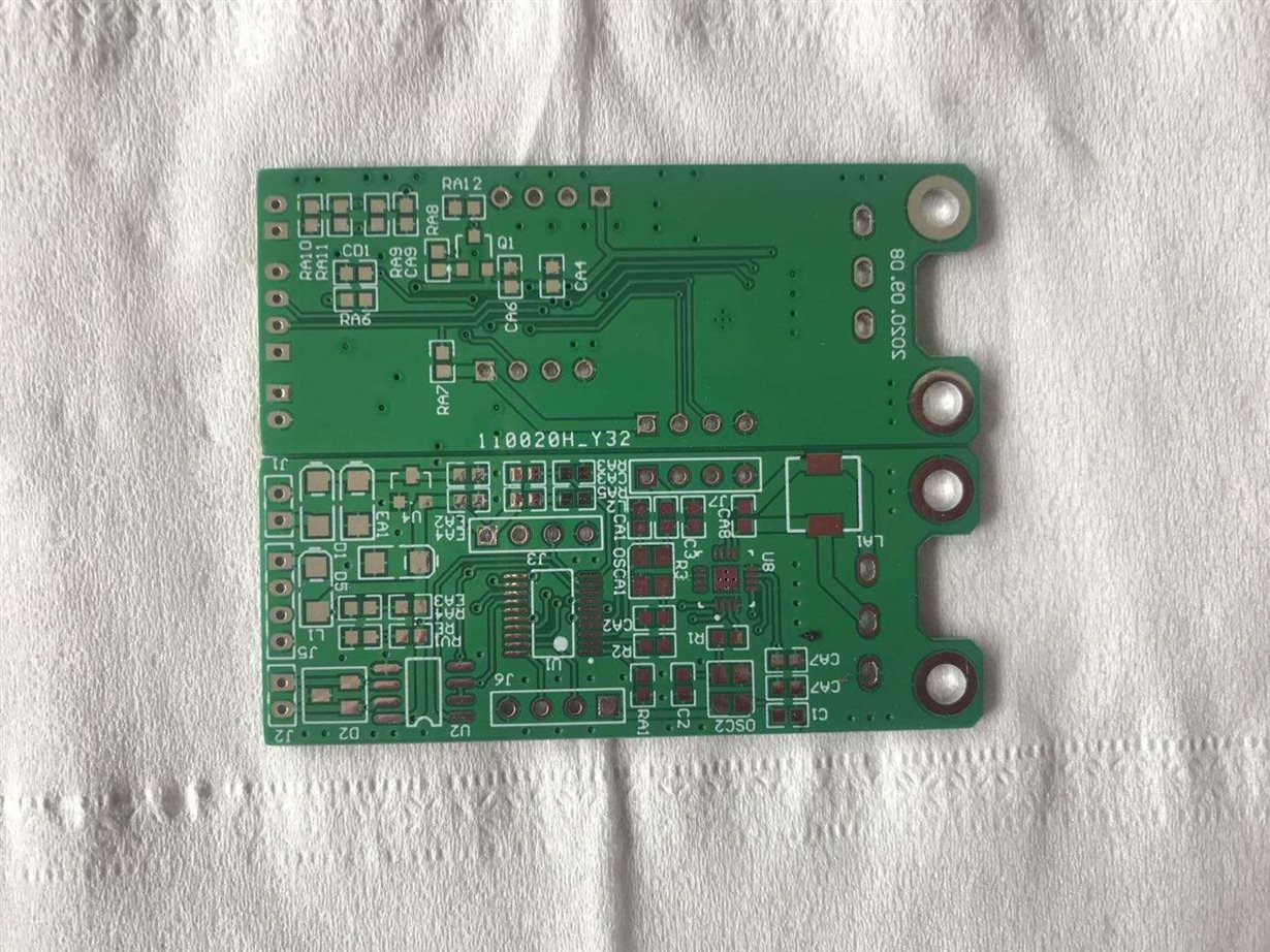
When using fdc2214, the external communication will be interrupted.

The cooling part on the back of the chip has been grounded. When touching the back of the chip by hand (unable to directly contact the chip, contact the PCB board on the back of the chip), the communication can return to normal.

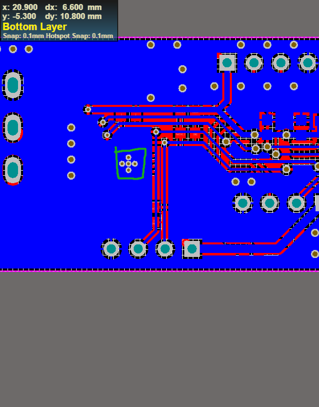
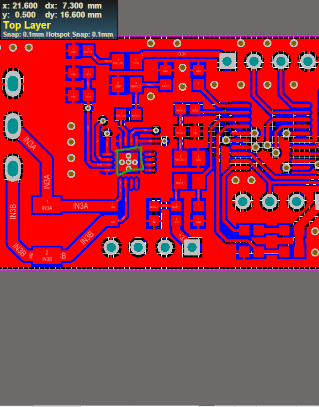
Now the chip schematic diagram and PCB layout board (marked with green circle) are sent up for your help.

  • Hello,

    I am sorry to hear that you are having issues and more information is needed and I can provide you guidance on the debug.

    Can you please clarify your statement by communication being interrupted ? Is the I2C communication not working ? or is the device chip not functioning as expected ?

    Can you probe the I2C lines with SDA and SCL and review what I2Clines look like ?

    You mentioned that when you put pressure on the chip the I2C communication works ? 

    Have you ensured that the IC is soldered professionally and no issues with the device ?

    Are there any shorts to Gnd ?

    Is the DAP of the FDC connected to the Gnd is yes, how are they connected ?

    Have you also tried to use our EVM and did you find similar issues ? 

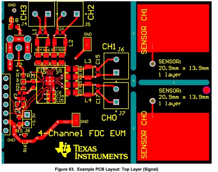
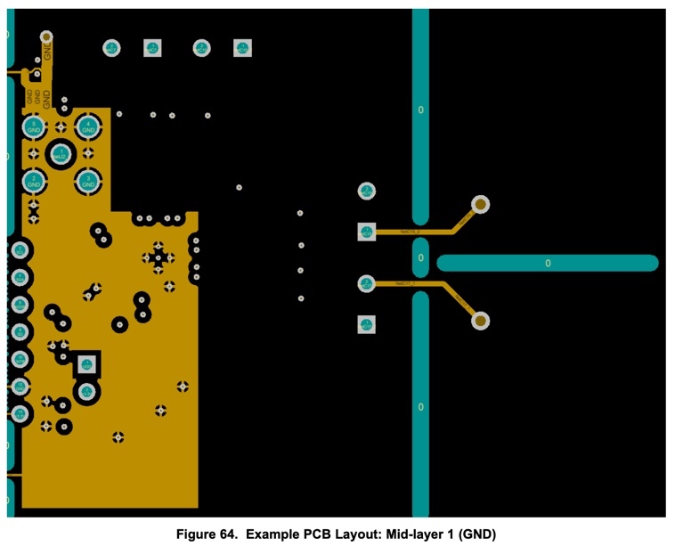
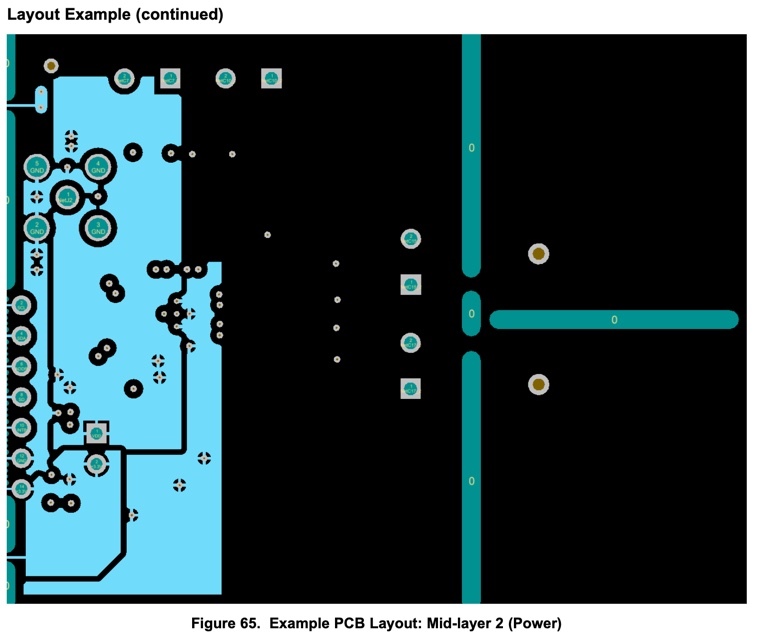
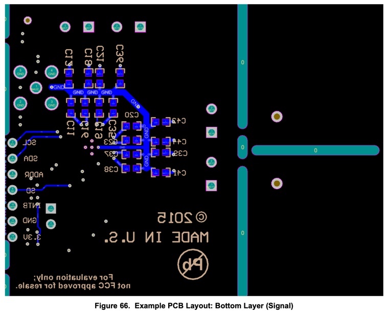
    In regards to the layout, I see that the board has not followed our guidelines in regards to capacitive sensing. We recommend that the Sensor inputs not have any planes around it as it can act as a parasitic capacitor. Its hard to say if the layout changes is causing the communication issues and certainly will have issues with the performance. 

    Here are the recommended pictures of the layout.