This thread has been locked.

If you have a related question, please click the "Ask a related question" button in the top right corner. The newly created question will be automatically linked to this question.

MMWCAS-RF-EVM: MMWCAS-RF-EVM

Part Number: MMWCAS-RF-EVM
Other Parts Discussed in Thread: MMWCAS-DSP-EVM, AWR2243, TDA2

Hi,

About the MMWCAS-RF-EVM, I have tow questions to ask,

1.  J3 - 20 GHz LO Debug Connector was not populated on the EVM board whether it will result in return loss  of 20GHz, then, the system performance will be affected ?

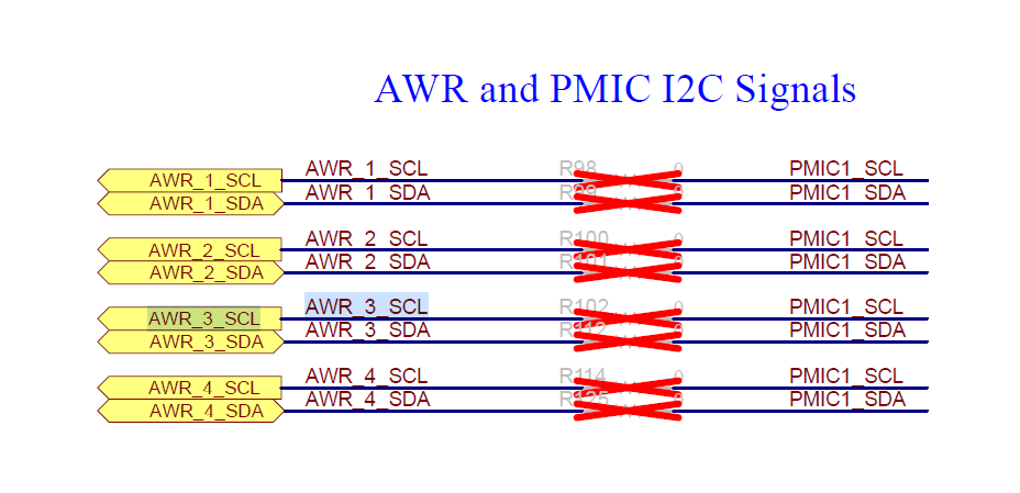
2. Why the only I2C slave address of master AWR2243 is configured by MMWCAS-DSP-EVM board ? how does the I2C slave address of other slave AWR2243s be configured to avoid addressing conflict ?

Thanks

Michael Su

  • Hi,

    The cascade team will review your question and get back to you later this week

    thank you

    Cesar

  • Hi Michael, 

    1. The two LO output on each device, FMCW_SYNCOUT and FMCW_CLKOUT, are two, independent PA paths. The J3 debug connector is routed to AWR #3, FMCW_CLKOUT and will not effect any of the other LO lines. 

    2. All of the I2C lines can be shorted together using the zero-ohm resistors found on page 9 of the MMWCAS-RF-EVM schematic. These are all mastered by the PMIC1 I2C port from the MMWCAS-DSP-EVM. 

    Thank you,

    -Randy

  • Hi Randy,

    Thanks for your reply

    1. The LO signal of AWR3 comes from AWR1 (master chip) through its FMCW_SYNCIN1 pin, then the LO signal is divided into two path:

         path 1 : does the x4 frequency

         path 2: output path 

       The J3 is connected to path2, so, when the J3 is not mounted on the board, the reflection will not affect the quality of  path1, is right ?

    2.  I know the four AWR chips share the same I2C bus, PMIC1 I2C, so, the four AWR chips should have different I2C slave address, but just the AWR 1 was

        configured  by DSP board via controlling the level of GPIO[0], [1], [2] pins of AWR1, but the others didn't, so, the others were configured by software ?

    Thanks

    Michael Su

  • Hi randy,

    Any update ?

    Thanks

    Michael Su

  • Hi Michael, 

    Sorry about the delay, I thought I had responded to this on 10/06, but I don't see my response! 

    1. Right, the RF x4 path vs. the LO output paths are totally separate and do not effect each other. 

    2. We do not support the I2C control path with mmWave Studio. Only SPI mode is supported. The GPIO are all routed to the TDA2 host processor though on the MMWCAS-DSP-EVM. So it should be possible to take the ProcessorsSDK examples and write an I2C GPIO address setup and controller. 

    Thank you,

    -Randy

  • Hi Randy,

    For the question 2,

    So, the control and configuration of AWR devices all are done by the SPi interface of TDA2, the I2C interface is not used for any control and configuration of  AWR devices ?

    In my view on the schematics of the TI EVM,

    the GPIO0 ~ GPIO2 of all AWR devices are connected to host-interface connector on MMWCAS-RF EVM, but  just the GPIOs of the AWR 1 are connected to TDA2 processor, the others are not on MMWCAS-DSP EVM,, it is so weird, but as the above statement said, the I2C interface is not used for any control and configuration of AWR devices, so, we should not care it, right 

    Thanks

    Michael Su

  • Hi Michael, 

    I see what you mean now. Yes, unfortunately, the MMWCAS-DSP-EVM does not route all of the GPIO to the TDA2 host. 

    The I2C interface is still a functional interface we support on the AWR2243 devices. It is perfectly valid to build up your own system to utilize this control path.

    The problem is our MMWCAS-DSP-EVM host board does not fully support it as an AWR control interface and mmWave Studio does not support it as an AWR control interface. 

    Thank you,

    -Randy

  • Hi Randy,

    Thanks for your reply

    Michael Su