This thread has been locked.

If you have a related question, please click the "Ask a related question" button in the top right corner. The newly created question will be automatically linked to this question.

TUSS4470: TUSS4470

Part Number: TUSS4470
Other Parts Discussed in Thread: , MSP-EXP430F5529LP, TDC1000, TDC7200, BOOSTXL-TUSS4440, TUSS4440

Hi guys!

i have some questions about TUSS4470 in order to know if it fits working with my application, one on the RX path and one on the TX path:

1) I saw the analog front-end in the receive path signal mounts a log amplifier, so the shape of the received echo signal is not so important as in TDC1000, but what matters is the TOF signal capture (I read that it is possible to capture echo signal with Vrms with magnitude of dozens of uVolts (maybe due to LNA input noise of the order of nV/√Hz). In the eval board BOOSTXL-TUSS4470 the analog output signal goes to the ADC MCU of the bottom board (MSP-EXP430F5529LP), and it’s shown in the GUI that the minimum resolution in TOF is 1uS, that means that lenght resolution in air is about 1 mm. It seems that this is a limit of the internal ADC (1 MHz), right?

So the question is: have the analog outputs VOUT (pin9) and the other digital signals outputs from internal comparators (OUT3, OUT4) a sort of other time discretization for example in the Sum stage or in other points, or can I consider a fully analog signal path with S/E output (like the LNA + PGA before the COMPIN in TDC1000 that worked so well)?

I mean i would like to know if e.g. is it possible to use one of the digital comparator outputs as a STOP signal for the TDC7200 IC without affecting its native time resolution below 1 nS? TDC1000 + TDC7200 worked so well in this sense so are there any issue on timing resolution using TUSS4470 + TDC7200?

2) My application needs high voltages because the transmission medium is air: concerning BOOSTXL-TUSS4470 can I reach hundreds of volts (obviously depending from the impedance seen by the transformer output at resonance frequency, but not the aim of this question in the hypothesis that is all optimized for the maximum power extitation) without using the external Pre-Driver Fets (not populated on board), but only the transformer drive or are Pre-Driver Fets mandatory for that aim (hundreds of Volts)? It seems the Trasformer Drive is only populated on the BOOSTXL-TUSS4440 right?

  • Hello,

    Sorry for the delay.

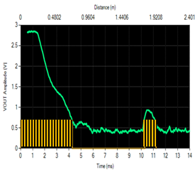
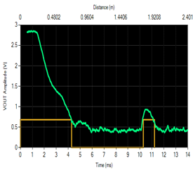
    Here is a depiction of VOUT with OUT3 and VOUT with OUT4:


    1) OUT4 would be better suited to be used as a STOP signal with the TDC7200. Given that you have an accurate START pulse, there should not be any timing resolution issues. With the programmable threshold, the TUSS4470 is more tunable in this sense, than the TDC1000. See datasheet section 7.3.4 for details on setting up OUT4 or OUT3. 

    2) Correct, only transformer drive with pre-driver MOSFETS is supported by the TUSS4470, and the direct transformer drive is only implemented on the BOOSTXL-TUSS4440 EVM. 

    Regards,

    Gabriel

  • Dear Gabriel,

    thank you for you support, referring to the previous numbering of questions:

    1)Thank you for your suggestion. So once confirmed that OUT4 is the best STOP signal for TDC7200, is there any difference in the analog chain AFE of the receive path between TUS4440 and TUSS4470 one should take into consideration?

    2) Glad to know i wasn't wrong. What I extrapolate from the BOOSTXL-TUSS4470 Scheme is that it is ready to be used without any transformer or FET, but directly from the internal bridge (max VDRIVE = 24 V of direct excitation on the transducer), but it could be used with 2 FETs by populating a zero ohm resistor in R7 and R10 and adding the external transformer  (to be ordered and mounted separately): this is the only way to have hundreds of volts on the secondary coil of the transformer.

    BOOSTXL-TUSS4440 is instead alredy ready for use with the external transformer, so it already has hundreds of volts in the transducer input (approximately plus or minus VDRV x TURNS RATIO of the transformer). So for my goal of having in the shortest possible time in developing a good hundreds of volt excitement the BOOSTXL-TUSS4440 seems like the best choice, right?

    3) Is there a safe procedure to activate the external VPWR MAIN VOLTAGE (5-36V) so as not to destroy the IC? I mean it needs to be applied after some register settings of the TUS4440, or is it enough to apply up to 36V on VPWR and then enable VDRV_HI_Z = 0, before the burst pulses in IO2?


    Regards,

    Federico

  • Federico,

    Yes, it sounds like the TUSS4440 is the right product to develop with. Definitely easier for driving a high voltage. The main difference between the devices is the driver and resulting frequency range supported. The receive paths are the same I believe. 

    Please see datasheet section 9 Power Supply Recommendations for supply and power up restrictions. The critical points are to have a stable supply, and to avoid hot plugging. I have not tested the device with an external higher voltage before, so let me confer with my colleagure on the high voltage operation, and I'll let you know tomorrow. 

    Regards,

    Gabriel

  • Thank you Gabriel,

    definitely TUSS4440 seemes the better choice in the range until 400 kHz,

    waiting for your last answer to confirm,

    Regards,

    Federico.

  • Admitting of not wanting to use an external VDRV, but internally adjusted from VPWR (which at this point VDRV can reach up to 20 V) is this the right way to proceed safely !?

    1) apply VDD = 5V
    2) waiting fot Tpwr_on = 10 ms
    3) apply VPWR = 36V (called MAIN BOOSTXL-TUSS4440 Schematic)
    4) enable internal regulation by writing VDRV_HI_Z = 0
    5) start Burst pulse for center tap excitation

    thank you.

  • Federico,

    Yes, that looks fine. 

    Just keep in mind that the VDD regulator output quality will largely determine the AFE noise floor and received signal SNR. 

    Also, see Table 21 for recommended components. 

    Regards,

    Gabriel