This thread has been locked.

If you have a related question, please click the "Ask a related question" button in the top right corner. The newly created question will be automatically linked to this question.

IWR6843: Understanding of IWR6843 timing diagram

Part Number: IWR6843

Hi Team,

I have few questions regarding IWR6843 Timing and Switching Characteristics.

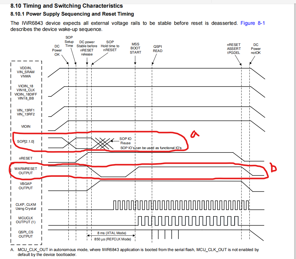
a) I have gone through the IWR6843 timing diagram, but I didn't understand, how this timing diagram is useful. I am trying to explore the people count project, how these SOP[2,1,0] pins are used. Here I am attaching a timing diagram screenshot with red mark identification for your reference. either we want to connect VCC or GND continuously to these SOP pins or is there any time delay. please give me a proper explanation for this.

b) With reference to the timing diagram, how WARMRESET OUTPUT pin is used. This pin is connected to 3V3 or GND continuously or any time delay we need to maintain. Can you elaborate? see the below screenshot for your reference.

Regards,

Srikanth 

  • Hello Srikanth,

        Above timing diagram provides power up sequencing activities. Few points to emphasize are:

    1) All the power supply need to be applied together.

    2) Device boot modes i.e. Functional mode, Flashing mode, Debug modes would be decided based on the SOP pins (TDO = SOP0, SYNCOUT =SOP1, PMIC_CLKOUT = SOP2) at the time of NRESET release. At this time device boot mode is registered and depending upon the device boot mode next set of boot activity would be carried out. 

    More details on this you could find from the below app-note

    IWR6843 Bootloader Flow https://www.ti.com/lit/an/swra627/swra627.pdf 

    3)  After the boot completion, SOP lines could be pin muxed as different functional pins based on the application program. 

    For the 2nd question more details could be found from the below E2E thread:

    https://e2e.ti.com/support/sensors/f/1023/t/969239

    Thanks and regards,

    CHETHAN KUMAR Y.B.