


art Number: PGA970
First of all we would like to bring to your attention the electrical schematic focusing on the LVDT PGA970 connection with the 5 wires LVDT/RVDT secondary side.
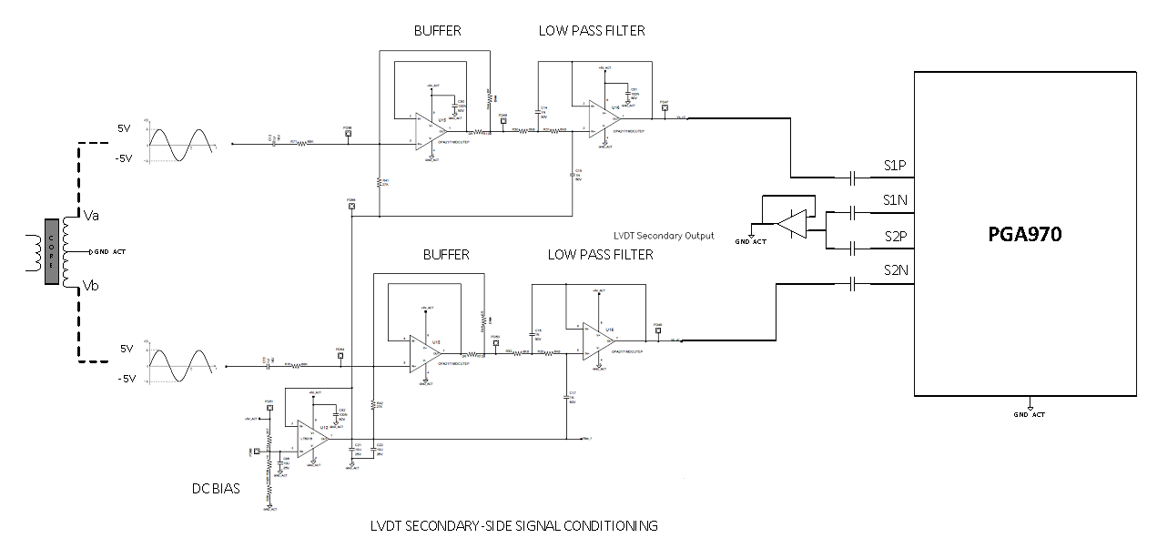
LVDT electrical specs are defined as follow:
• 7Vrms excitation (20Vpk-pk on the primary side10Vpk-pk each signal on the secondary side)
• Fex: 3000Hz
As per the above schematic, the LVDT secondary-side signals are properly filtered and partitioned to achieve the PGA970 ADC Input Dynamic (Vrefmax: 2.5V).
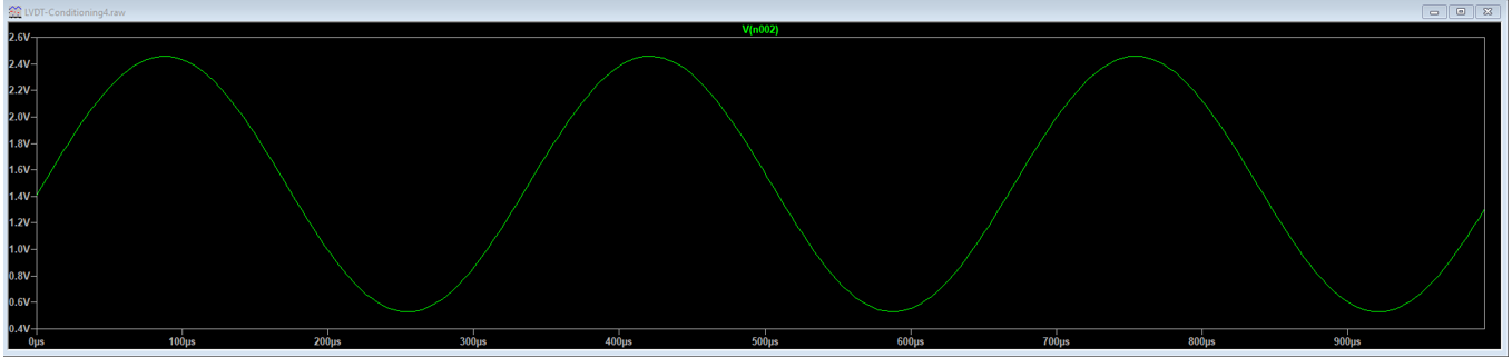
The dynamic of the secondary-side signals thereafter becomes about 2.4Vpk-pk with an offset equal to 1.5V. The simulation results are shown below:

We would like to know:
- Is this the right connection for a 5-wires LVDT/RVDT?
Regarding the SW side we intend to use the PGA970 in RESET MODE and access the data via SPI link (ARM M0 is in RESET MODE).
We would like to know:
- How can we set S1_S2_CFG ->BIAS_VCM_CONTROL?
- Based on our conditioning front-end circuit, how can we set S1_CFGàS1_GAIN and S2_CFG S2_GAIN?
- How can we set S1_CFG->S1_SEM and S2_CFG->S2_SEM

