This thread has been locked.

If you have a related question, please click the "Ask a related question" button in the top right corner. The newly created question will be automatically linked to this question.

PGA970: 14-bit DAC look-up table (LUT)

Part Number: PGA970

Hello Scott

I'm running my LVDT/RVDT 5 wire application using PGA970 integrated in my custom board.

I was able to configure all registers to setup correctly S1 and S2 demodulation channels when arm M0 is in reset via SPI.

The last step is to understand how to configure the Waveform Generator.

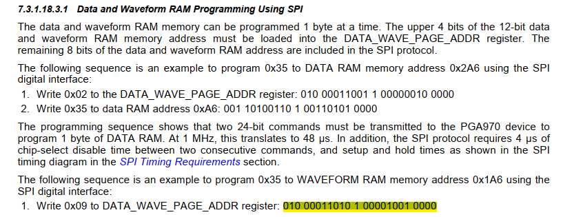
I wouldn't write via SPI the Waveform data RAM at each powerup, it would mean to write the DATA_WAVE_PAGE_ADDR register to 8 and then write each data Waveform RAM location reserved for the samples.

My primary excitation should be 3kHz (0x52 samples are needed for the quarter sine wave period).

The alternative scenario is to use the 14-bit DAC look-up table (LUT). I inspected the demo software:

   /*Read waveform table size*/
   FRAM_DATA_Read(1,WAVEFORM_TABLE_SIZE_OFFSET,&Waveform_Table_size);
   memcpy((void *)waveformTable,(void *)(FRAM_DATA_START_ADDRESS + WAVEFORM_TABLE_OFFSET),Waveform_Table_size);
 
FRAM_DATA_Read() retrieves the size of the quarter sine wave period, in my app it should be 0x52. 
memcpy moves samples from FRAM address ((0x00001800 +0x600)) to RAM address (20000800).
 
In the case of I would like to run PGA970 having no firmware on board in reset mode, could I load the samples in the FRAM LUT table and then check periodically the Waveform RAM? 
 
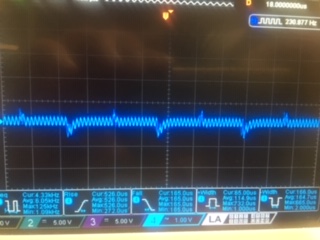
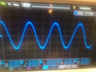
I did some tests in order to verify that Waveform samples are really saved in RAM by generating a quarter of a waveform via software having F = 3kHz and 
then reset the PGA970 via SPI. I queried via SPI the Waveform Ram (writing first DATA_WAVE_PAGE_ADDR = 8 and then reading RAM memory locations sending first message 001 00000000 0 00000000 0000B = 0x200000H) but I hadn't the expected results i.e I didn't read first sample of the waveform.
 
Note: I measured the correct amplitude and frequency of the waveform with an oscilloscope.
 
Thank you 
Carmine Ricca
 
  • Hi Carmine,

    Are you finding that you have trouble with the waveform RAM not being set correctly in any case? Or is the problem when you write to the FRAM LUT expecting the waveform RAM to have the corresponding values stored at powerup?

    What values do you see, or is it empty?


    Regards,

  • Hi Scott

    I'm focused on the generation of the Primary LVDT excitation for our purpose it should be:

    • 3kHz Sinewave (Quarter Wave Length 83)
    •  LVDT Differential mode
    •  Differential Gain 1.67V/V
    •  Differential VOCM 0.75 V
    •  DAC VCM 0.82V

    First of all I set  MICRO_INTERFACE_CTRL to 0x03h (to select DIG_IF and to reset PGA970).

    I implemented a for loop to send 83 x 2 bytes

    I report the pseudo-code implemented into an external micro connected via SPI with the PGA970 device

    /* set ADC_EN_VREF_BUF and NO_SHUT_DOWN of ALPWR */

     message = ALPWR | WRITE | ADC_EN_VREF_BUF;
     message &= NO_SHUT_DOWN;
     response = SendMsg(message); //message is 0x4A1040
     
     /* Set WAVE_EN to 0 of WAVEFORM_GEN_CTRL*/
     message = WAVEFORM_GEN_CTRL | WRITE;
     message &= WAVE_DIS;
     response = SendMsg(PGA970_Cmd);//message is 0x4F1000
     

    for(i=0; i < PGA970_WAVEFORM_LENGTH; i++){


    SendMsg(0x433080u)//Set WAVE_PAGE_ADDR 0x8 -> RAM addr 2000800 starting address

    //Send via SPI msg:         001     |  Addr    | Write     | Byte

    SendLSB_Waveform_Data ( 0x20000000 |( i << 13) | (1 << 12) | (LSByte[i] << 4));

    SendMSB_Waveform_Data ( 0x20000000 |( i + 1 << 13) | (1 << 12) | (MSByte[i] << 4));

    CheckData[i] = ReadData(); // Data have been set correctly: what I write is what I read

     message = WAVEFORM_TABLE_LEN | WRITE | (0x52 << 4);
     response  = SendMsg(message); // message is 0x4F5520
     
     message1 = WAVEFORM_DAC_OFFSET_1 | (0x08 << 4) | WRITE;//(LS Byte) 0x4F9080
     message2 = WAVEFORM_DAC_OFFSET_2 | (0x2C << 4) | WRITE;//(MS Byte) 0x4FB2C0
     response = Send2Msg(message1, message2); // response is 0x05082C
     
     message = (LVDT_OP_CTRL | WRITE | SKIP_FILTER_ENABLE | LVDT_GAIN_CTRL_1_67_V_V);
     message &= LVDT_SINGLE_DIFF_MODE;
     message &= DIFF_VOCM_CTRL_0_75_V;
     message &= DACVCM_CTRL_0_82_V;
     response = SendMsg(message); // message is 0x479700
     
     message  = AMUX_CTRL | WRITE | (((1 << 0)|(1 << 1)|(1 << 2)|(1 << 3)) << 4);
     message  = SendMsg(PGA970_Cmd);//message is 0x4C90F0
     
     message = LVDT_LPBK_CTRL | WRITE;
     message &= DIS_LOOPBACK; // ~((1 << 0) << 4)
     response = SendMsg(message);// message is 0x47B000

     message = WAVEFORM_GEN_CTRL | WRITE | WAVE_EN;
     message = SendMsg(message); //message is 0x4F1010
    For my implementation I used as ref the 7.5.6 section ofSLDS201A Jan 2016
    In the picture below you can see the profile detected by the oscilloscope:
      
    In this other picture you can see what kind of profile PGA970 software demo on board is able to generate using the same register settings:
    Probably I forget some detail but I followed step by step 7.5.6 section and I crosschecked the the PGA970 software demo implementation. What am I doing wrong?
    As second solution I tried also successfully to write FRAM LUT starting from the 0x00002400 address,  but I wasn't able to generate the primary output tone.
    Thanks in advance Carmine Ricca


  • Hi Scott

    I'm working hard in order to generate the Primary excitation.


    It doesn't match with the Register  DI and offset: 

    DI = 0x2

    Offset = 0x19

    010 00011001 1 00001001 0000

    the bit 13 and 14 are swapped.

    What have i consider correct?

    In order to write Waveform RAM memory filling it with 83 samples (Quarter wave), considering that starting address should be 20000800, what address page should I use (0x08 0r 0x09)?

    We would like to use in our application the PGA970 but this issue is the last obstacle thank you

    Carmine

  • Hi Scott

    Finally I fixed the technical software issue: I indexed wrongly the For loop because I used uint16 instead of uint32 index i type that corrupted the shifted left  13 instruction.

    I erased the demo program completely in the PGA970 and then I run my external micro in order to configure all registers via SPI. I was able to write DATA_WAVE_PAGE_ADDR_8 and all RAM location reserved for the quarter sine wave samples.  Finally 3kHz sine wave has been successfully detected with an oscilloscope.

    Now we are confident that PGA970 could be the candidate as demodulation subsystem of our application

    Thank you


  • Hi Scott

    System is working fine, I would like to understand LUT functionality. I'm able to write correctly the waveform samples into the FRAM starting from 0x000800 + 0x600 (I checked via CCS the FRAM it' ok) further I'm able to write wave length at the 0x000812 FRAM location (as reported in the sw demo). When I put the PGA970 in reset the primary output is always down. 

    is LUT available only when firmare is running?

    Thanks

    Carmine

  • Hi Carmine,


    Yes, the LUT values are moved from the FRAM into the waveform RAM on powerup through firmware in most cases, although it could also be done through the digital interface by reading them out from the lookup table and writing them back to the RAM.

    Regards,