This thread has been locked.

If you have a related question, please click the "Ask a related question" button in the top right corner. The newly created question will be automatically linked to this question.

A/D Recommendation for Low Power Operation with 3 DRV425

Other Parts Discussed in Thread: TPS63900, ADS8363, DRV425, ADS8867, TMUX1109

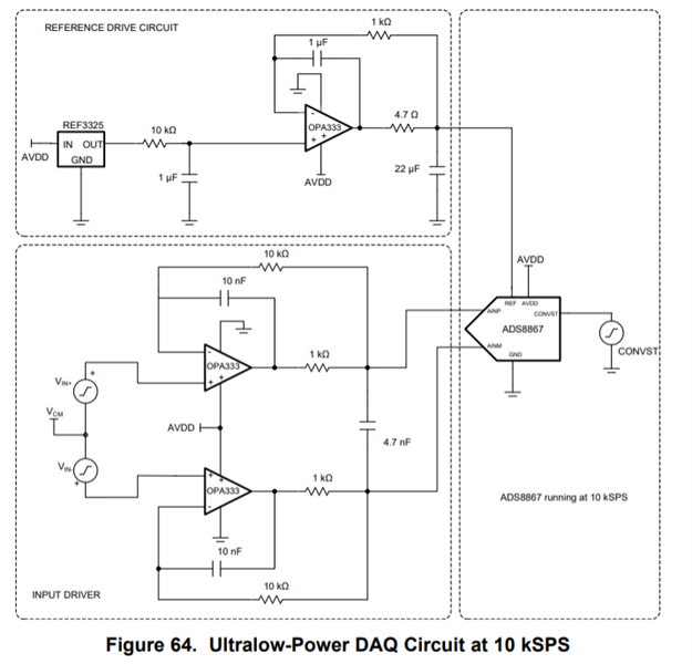
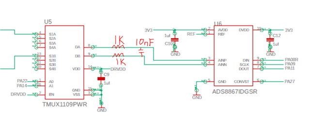
Given a battery powered application with a low standby current of 20uA, we want to add 3 DRV425s with an SPI A/D. We plan on adding a TPS63900 to get 3.3V for the system with a software controlled power switch for the A/D and DRV425s. The challenge has been to find a low power solution that will give us all 3 DRV425 data at a 500Hz rate. We haven't found an A/D solution for the turn on and convert time with 3.3V operation. The ADS8363 looked good but the turn on time is like 4ms. We looked at keeping the A/D on all the time but assuming we understand how the part works, it is about a 1ma when idle. The A/D should have 3-4 channels of pseudo differential input, 16-bit, SPI, 3.3V for analog/digital interface and low power without conversions.

Please recommend an A/D that might work or a better system solution.

Best regards, Alan

  • Hi Alan,

    Please take a look at ADS8867.  It automatically enters power-down mode after the conversion finishes.  At 2ksps rate (500sps x4 channels), the average supply current will be around 4uA.  It does not include a multiplexor, but TMUX1109 would be a good fit to support 4 differential inputs.

    The main source of quiescent current will be the reference/buffer circuit, which will need to stay powered unless you can tolerate a 10mS or longer power-up time.  Take a look at Figure 57 in the ADS8867 datasheet for a recommended reference that can support up to 10ksps.

    Regards,
    Keith Nicholas
    Precision ADC Applications

  • Hi Keith,

    Good suggestions, how do I attach a schematic for the following questions:

    1. How does the 3V3 and DVRDD look with regards to leakage? In particular the TMUX part to the A/D input.

    2. On the DRV425, what values for the filter and shunt resistor, or how to calculate them?

    3. Any other inputs or recommendations appreciated.

    Note, only one DRV is illustrated on the schematic, I'll add a second and possible a third later.

  • Hi Alan,

    In order to insert a schematic image,  click on 'Insert', and then choose 'Image/Video/File'.  On the browse window, double-click the 'Upload' text, then select a *.png image file to upload.  I also suggest increasing the 'Dimensions' values (640x480 or 800x600) to increase the resolution of the schematic image.


    Please post the schematic and I can comment on question 1.  Regarding question 2, an output RC filter of 1kohm and 10nF should work well.

    For specific questions using the DRV425 (shunt resistor), please create another E2E post specifically for DRV425 so the appropriate support team can help answer.

    Thanks

    Regards,
    Keith

  • Hi Alan,

    The image still did not load.  There is an easier way (I just discovered); drag the *.png image file and drop it into the text window.  

    It will insert the image in low resolution, but you can click on the image and adjust the resolution to something higher such as 800x600. 

    Below is an example out of the ADS8867 datasheet.

    Regards,
    Keith

  • Hello Alan,

    I suggest keeping the TMUX powered directly from the 3V3 supply.  The supply current is less than 1uA. 

    You will want to move the filter from the input of the mux to the output of the mux and keep it in a differential configuration.  1k resistors and a differential 10nF cap will still allow for sample rates up to 4ksps.

    Regards,
    Keith