Hi
I am now looking at and designing Altium data and documentation provided by TI.
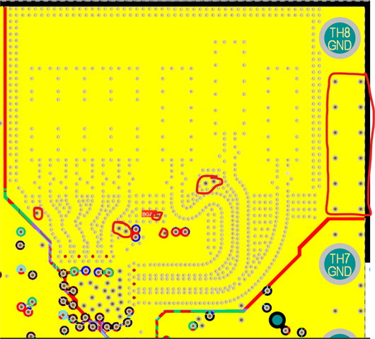
In the design document it is written:
"note very important L1, L2, L4, L6 grounding, through VIAs"
This document is HardwareDesignChecklist_V0p8.
I want to know exactly what that means.
Does this mean that the VIA is connected to Layers 1, 2, 4, 6?
Also, I would like to know exactly where the VIA is in the Altium data.
i waiting for your answer.
Thanks.