This thread has been locked.
If you have a related question, please click the "Ask a related question" button in the top right corner. The newly created question will be automatically linked to this question.
Hi,
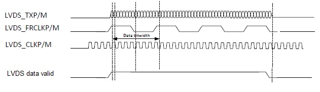
In AWR1243 datasheet, I can't find detail info of pin definition for LVDS. In AWR1443 EVM schematic, I found HS_DEBUG1 is for LVDS_FRCLK and HS_DEBUG2 is for LVDS_VALID.
I found a LVDS timing in Figure 13-5. LVDS Interface Timings of swru520.pdf (awr14_16_trm), but there is no info about LVDS valid signal. Would you pls kindly advise the timing of LVDS Valid?
Vivek,
My customer wants to have a signal to know when the ADC frame starts and ends. Can the LVDS data valid to show such info? Will it continue to be active during the whole adc/chirp frame data transfer?
I draws a timing of lvds data valid signal as below. Would you pls help to check if it is correct?