This thread has been locked.

If you have a related question, please click the "Ask a related question" button in the top right corner. The newly created question will be automatically linked to this question.

LMG2100R044: Dual-Phase 500-kHz 40-A Synchronous Buck Regulator with LM5148

Part Number: LMG2100R044
Other Parts Discussed in Thread: LM5148, LMG3100R044, PMP23392

Tool/software:

Hello TI,

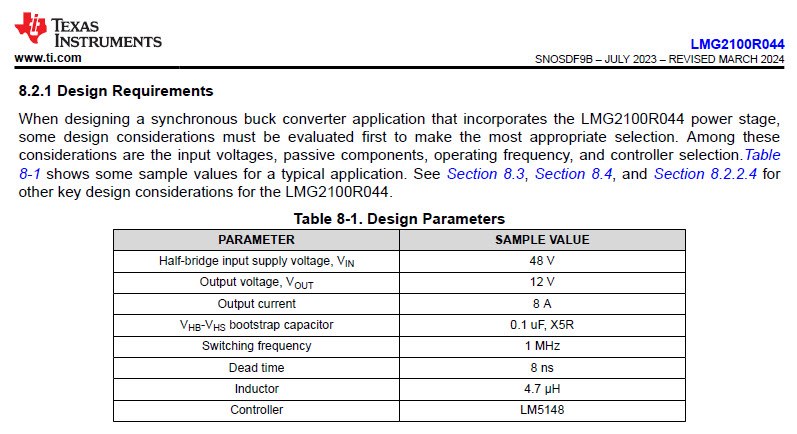
On this moment we are into a design of a Dual phase 500kHz 40 A synchronous Buck regulator, with a voltage input range from 19.2V to 52V and a total power of 40A at 12V output.

For the Buck regulators, we will use into dual-phase mode, two pieces of LM5148 and two pieces of LMG2100R044.

We already noticed that the SW pin of the LM5148 should connect to PGND, but maybe there are settings needed to have the correct connection to the GanFet LMG2100R044.

Are there constraints into this combination and do you have a recommended circuit diagram?

Can we make use of the internal LDO 5-V VCC of the LM5148 to supply LMG2100R044?

Best regards,

Stephan

  • Hello,

    Thank you for reaching out, I can share some recommended practices and constraints with this connection but need some time to write up.
    Please allow till tomorrow for a full description.

    Thanks,
    Zach Soviero

  • Hello Zach,

    Please take your time, we want to do it right.

    On this moment we do want to prepare prototype and now I do working onto the calculation and Circuit diagram of the power supply.

    best regards,

    Stephan.

  • Hello Stephan,

    As you pointed out, there is an issue when pairing LM5148 to LMG2100 because LM5148 is designed to work with discrete FETs that have no integrated gate driver, therefore leveling shifting circuitry is included.
    LMG2100 also includes level shift circuitry, which is the problem I was investigating for you

    I wanted to confirm what other connections (if any) were needed other than the one you pointed out: connecting SW of LM5148 to LMG2100 ground. Although instead of PGND, connect this to AGND of LMG2100.
    AGND and PGND are referenced together, but we use AGND as a quiet ground for digital/control signals that does not see interference noise from high power main power loop PGND. AGND is shorted to PGND inside of LMG2100 so both grounds are connected with a kelvin connection.

    There are no other physical connections needed, however, connecting SW of LM5148 to AGND has some trade-offs. There are features integrated in LM5148 that use SW referenced signals such as adaptive deadtime, soft startup, etc. Therefore, connecting SW to AGND will cause these features to be disabled, and the controller will act more like a traditional PWM controller. You may have already been aware of this point, but just including for your reference.

    Thanks,
    Zach Soviero

  • Hello Zach,

    Many thanks already for this update.

    When I look into the datasheet SNOSDF9B_July_2023_revised_March 2024 of part LMG2100R044 at page 15.

    I see that the controller is the LM5148 and the Dead time is 8nS, is this the minimal set value of the LM5148?

    Please can you clarified more which integrated features in LM5148 that use SW referenced signals  will be not working when we do connection to AGND ?

    Is this still a good controlled combination LM5148 to LMG2100R044, into a high power combination.

    Or should we connect the SW reference signal of the LM5148 at SW pin LMG2100R044 and design a level shifter behind the HO output of the LM5148 to the right level of HI of the LMG2100R044?

    We want to use the pro's of the LMG2100R044 GaN FET, but the control need to be into a save operation area.

    As the controller LM5148 is used into this datasheet of the LMG2100R044, is there maybe a reference circuit diagram of this combination at TI team?

    Did TI team build this combination and tested it?

    Best regards,

    Stephan

  • Dear TI team,

    Do you have any Update, to my questions?

    Best regards,

    Stephan

  • Hey Stephan,

    Apologies for the delay, I can still help answer some more details, but I need to pull in the controllers team to help label exactly all of the features that work and do not work when pairing LMG2100 and LM5148 together

    I do know that the deadtime will not be 8ns, please disregard this section of the datasheet as we are working to update it. Normally the buck controller will use adaptive deadtime control, but this feature is turned off when connecting SW to GND, so deadtime will default to 100ns I believe.

    This is a very suitable controller to pair with LMG2100, and we have a reference design using it: PMP31349
    Additionally, we have a reference design using two single GaN devices in a half-bridge configuration with LM buck controller: PMP23392
    P
    lease take a look at the test report for both reference designs as they will have some additional information

    Thanks,
    Zach S

  • Hi Stephan,

    By utilizing the LM5148 and the LMG2100 together - the main change that you are doing in the controller operation is connecting the SW to GND which disables the Deadtime circuitry of the controller. The deadtime will now be managed by the GaN device. I don't think any other functionality will be affected by this implementation (as can be seen by the Functional Block Diagram as well).  

    As Zach shared earlier, you can look at the https://www.ti.com/tool/PMP23392 which is a proven design and seems to be very similar to your requirements. The test results of this design are also available in the above link.

    Does that answer your question or do you need more information? 

    Thanks,

    Best Regards,

    Taru

  • Dear TI-team,

    Many thanks to your support.

    best regards,

    Stephan

  • Hi Taru,

    I am colleague of Stephan.Based on your feedback on dead-time control circuitry, i think it makes more sense to use the LMG3100R044 GAN device. With this device it is possible to connect switch-node in normal way, so the adaptive dead-time functionality is still operational. (like in the PMP23392 example)

    Another possibility that i would like to confirm is possibility of hybrid Mosfet/GAN DC/DC. Based on calculator it seems to make sense to use GAN device for top switching device and normal Mosfet for bottom device. This minimizes switching losses in top device and conduction losses in bottom device. I can't think of any reason why this would not work, but i would like to confirm with TI experts I am not missing something. It is also very cost effective solution because Mosfet is much cheaper for same RDson performance compared to GAN.

    best regards,

    Tom

  • Hi Tom,

    Theoretically, this should work (however, let me confirm this internally with the designers of this reference design).

    Thanks,

    Best Regards,

    Taru