CDCLVD1213: CDCLVD1213 : Can it support 480MHz 0dB input clock

Part Number: CDCLVD1213


Hi Team,

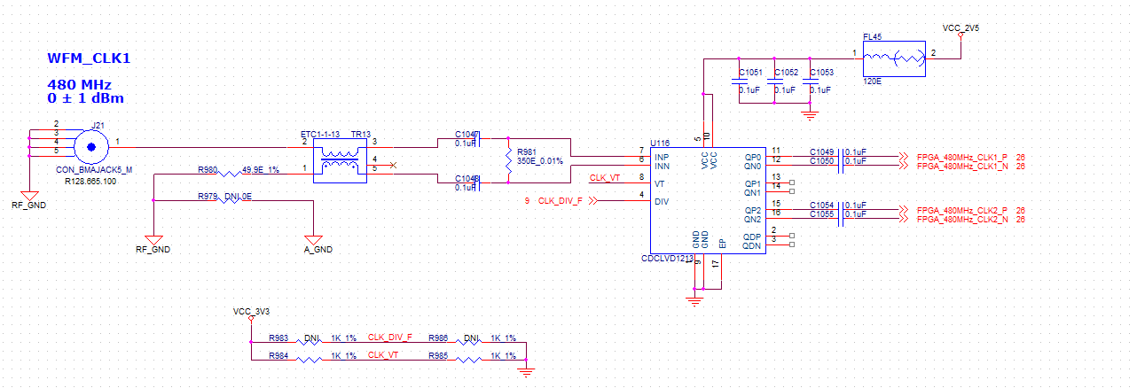
I am receiving a 480 MHz, 0 dBm signal from an external board, which needs to be split and fed to both the DAC and FPGA on my board.

As per the CDCLVD1213 datasheet, the supported input amplitude range is 0.3 Vpp to 1.6 Vpp. I would like to confirm whether my attached schematic meets this requirement.

If not, please suggest an alternative part that can support this specification.

Kindly do the needful.

image.png

  • Hi Varun, 

    I believe CDCLVD1213 should be suitable for this application. 0dBm corresponds to about 630mVpp going into a 50 Ohm load which should be sufficient here. The balun will probably have some insertion loss but it should still be meet the 0.3 Vpp minimum input requirement. 

    Also just out of curiosity, why was the 350 Ohm termination chosen for R981? We generally recommend a 100 Ohm termination for LVDS for best impedance matching. 

    Regards, 

    Connor