This thread has been locked.

If you have a related question, please click the "Ask a related question" button in the top right corner. The newly created question will be automatically linked to this question.

TS5A23159: Question about Pin Capacitance - Cnc(on) / Cno(on) / Ccom(on)

Part Number: TS5A23159

The Datasheet specs CNC(ON), CNO(ON), CCOM(ON)

[1]
Assuming a signal gets routed from [Host] -> [NO->COM] -> [Device]; will the signal see rise-times that relate to the combined CNO(ON)  CCOM(ON)?

[2]
Basically, the bus capacitance would be the combined NO/NC + COM capacitances, right? (55pF + 54.5pF)

[3]
Is this capacitance between the signal line and GND?

  • Hi Darren,

    You do not add the capacitances together. On Capacitance is the measure of capacitance to ground when the switch is on. This is why there is a large jump between off capacitance and on capacitance typically because the conductor surface area becomes larger when the switch is closed. 

    I will say this datasheet is a bit confusing because on the 5V supply case they are different values - and to be safe its better to assume the larger of the two - but they are referring to the same capacitance. 

    For your specific questions:

    1. Signal rise time is a mix of the transition time + the RC charge time of the multiplexer's output. If the switch is already NO -> com and there is no load attached the rise time is simply a RC charging circuit where the time constant is  R_on * C_ON. However when the signal is switched from NC to NO there is also the Toff and Ton time that come into play. However if the mux output is not just its output capacitance than the output voltage rise is going to be more dependent on the load instead of the multiplexer. 

    2. No use the largest one to be safe - The off to on capacitance for the NC/NO side wouldn't jump ~3x if it didn't include the drains capacitance + any capacitance of the closed switch itself.

    3. Yes these capacitors are from I/O lines to Ground.

    If you have any other questions please let me know!

    Best,

    Parker Dodson

  • Hi Parker,

    Let me confirm two points, if you are able to answer.

    1) The capacitances for NO/NC/COM when ON or OFF come from actual measured values, as shown in Figure 17 of TS5A23159 DS, right?
    These values were measured, as opposed to being calculated, due to the complexity of the transistor network internal? (DS doesn't have any functional block diagram showing MOSFET/Transistor setup on how the pins function)

    2) The 55pF and 54.5pF difference...it looks like COM's C is lower than NO/NC's. Makes me think going through the internal transistors/etc structures from COM to NO or NC, you add ~0.5pF. Does that sound about right?

  • Hi Darren,

    1. Yes the capacitance values are measured - they are not calculated. 

    2. Hi Darren - yeah that sounds about right - this deviation only occurs at our 5V spec'd range so this is something that should only be a concern at higher voltages (5V) as this spec is equivalent for lower ones. 

    Best,

    Parker Dodson

  • Hi Parker,

    Quick follow-up, can you provide (offline?) any equivalent circuit of such an Analog Switch? 

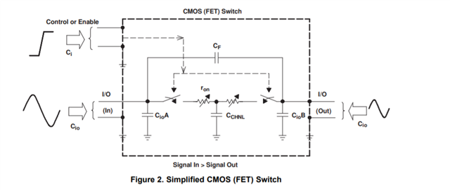
    I'm looking at Fig. 2 from here: https://www.ti.com/lit/an/szza030b/szza030b.pdf

    Does that kind of describe the setup, and how the capacitances are related...?

    Darren

  • Hi Darren,

    The referenced literature figure 2 is a correct model of a switch. 

    However for application sake - the model is simplified to a behavioral model. 

    C_IOx - this is the  capacitance to ground of that I/O pin - it is also known as the "OFF CAPACITANCE" typically on larger configuartions (2:1, 4:1 , 8:1 etc.) the drain off capacitance is going to be larger because it has a larger area. The C_CHNL is the channel capacitance of the mosfet(s) that are used as the switch.  Cf is the feedthrough capacitance that high frequency signals can bleed from input into the output.

    When the switch closes Cf can be neglected, the switch pathway can be accurately modeled as an RC circuit. Where the R is the on resistance of the channel and the C is the combination of C_IOA + C_CHNL + C_IOB = C_ON. 

    If you still want me to follow up with you offline please let me know - I didn't go straight offline because this information that we put out so its okay for us to share our published stuff. 

    Best,

    Parker Dodson