This thread has been locked.

If you have a related question, please click the "Ask a related question" button in the top right corner. The newly created question will be automatically linked to this question.

SN74CBTLV3253: Our project use TI SN74CBTLV3253 and found some abnormal symptom

Part Number: SN74CBTLV3253


Hi ,

It is Jon from Inventec sever team.

Now we found the symptom need your support.

Our project use TI SN74CBTLV3253 and found some abnormal symptom.


As SPEC logic diagram below pig1,

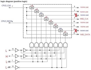
When S1 = H (3.3V), S0 = L (0V), force turn on internal two SWs, 1A = 1B3, 2A= 2B3.

We found the 1A pick up some noise from 1B4, and 2A pick up some noise from 2B4 such like below waveform capture. The noise around 150mVp-p above as pig2.

Is it reasonable and why?

Or other solution can reduce the noise. Please advise.  


  • Hi Jon,

    This phenomenon is related to the parasitic capacitances of the switches inside the device where they couple the input signal of the off channel to the output depending on the frequency. The lower the frequency, the less this effect happens as the capacitance has a much higher impedance at lower frequencies. As you increase frequency, this effect increases and will see more of the signal on the output.

    This effect is also increased by the layout of the board. If poor board layout techniques are followed and you increase your output resistance, you will see a higher portion of the signal on your output as well. So what you are seeing is definitely a reasonable possibility depending on how the board layout is and loading conditions.

    Thanks!

    Bryan