This thread has been locked.

If you have a related question, please click the "Ask a related question" button in the top right corner. The newly created question will be automatically linked to this question.

TMUX1209: Internal equivalent circuit

Part Number: TMUX1209

Hello expert,

My customer is evaluating TMUX1209.
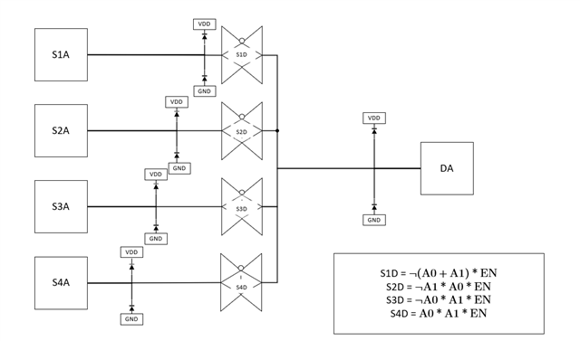
Then, they observed100mV as high impedance on DA/DB during EN=0.
I guess it is from internal protection diode or something but there isn't any explanation regarding this on datasheet.
Therefore, would you provide internal equivalent circuit for confirming reason of this 100mV during EN=0?


Best regards,
Kazuki Kuramochi

  • The absolute maximum ratings imply that there are ESD protection diodes from GND to DA/DB and from DA/DB to VDD.

    When the I/O pins are in the high impedance state, they are floating, i.e., it is not possible to measure their voltage. That 100 mV value is an artifact of the measurement process.

  • Hi Kazuki,

    Clemens is correct - when EN = 0  the output (DA/DB) is disconnected from the inputs via a high-impedance stage. If the output (DA/DB) is disconnected from the a load and you are just measuring the pin w.r.t. ground it is a floating voltage and cannot get an accurate reading.

    The structure can be shown as the following:

    This shows one of the 4:1 multiplexers in the TMUX1209. They are relatively simple devices there are ESD protection diodes on the I/O as shown. The switch structure is an analog transmission gate - the state of which is dictated by the logic equation in the figure above. If the equation renders a 0 the mosfets, which with EN = 0 it always will,  within the transmission gate are going to be in cut-off (high impedance) - and with no defined voltage on the D pin for the test the diodes are essentially open circuits.

    If you have any other questions please let me know!

    Best,

    Parker Dodson