This thread has been locked.

If you have a related question, please click the "Ask a related question" button in the top right corner. The newly created question will be automatically linked to this question.

SN74CB3Q3253: SN74CB3Q3253 question for OE and output pin.

Part Number: SN74CB3Q3253


Hi Team,

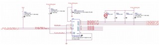
Customer would like to use SN74CB3Q3253 to replacement as below schematic, they have concern as below:

1. they found that VCC recommend 2.3V~3.6V in spec , therefore , if they want to change to pop this component , they need to modify VCC and OE pin PU rail (change to 3v3 ) , right?

2. Does the output pin need to PU resistor or not?

Regards,

Mark

  • Hi Mark,

    1) Yes, they will need to modify the rails used for this device to properly function. As you mentioned, the SN74CB3Q3253 works within the 2.3-3.6V range and the circuit needs to be altered to accommodate this. In addition, the OE pin has a VIH level of at least 1.7V if you are using a 2.3V-2.7V supply and 2V if you are using a 2.7V to 3.6V supply. So depending on which supply rail you use, you can either keep the current OE pullup of 1.8V if you are using a lower supply rail, otherwise you will need to modify that rail if you are using a higher supply rail.

    2) It is recommended for JTAG to utilize pullup resistors. For muxes like this, it is also recommended to have pullup resistors on both sides (which is what you already have) to ensure the communication signals are always in a defined state.

    Thanks!
    Bryan