

Other Parts Discussed in Thread: TS5A2066, SN74LVC2G66

This thread has been locked.
If you have a related question, please click the "Ask a related question" button in the top right corner. The newly created question will be automatically linked to this question.
Hi Aswin,
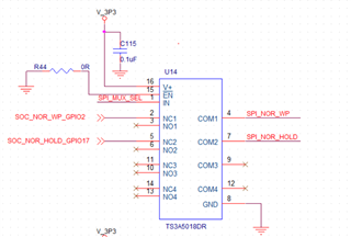
Please see the table below for your schematic:
| PIN | COMMENT | ACTION REQUIRED |
| 1 - IN | If IN is ever left floating - an undefined logic state can occur and output will be undefined with an increase in supply | If this pin is ever left floating a pull-down or pull-up resistor can ensure a defined logic state. If the Pin is not ever left floating No Action Required |
| 2 - NC1 | Signal SOC_NOR_WP_GPIO2 should be between 0V and 3.3V during Operation (3.3V supply) | No Action Required |
| 3 - NO1 | Analog I/O pins left floating on the multiplexer can cause reflections at higher frequencies. For lower Frequency operation it can be left floating (this is relative to solution size) | Best Practice is to terminate to ground with 50 Ohm resistors - but lower frequency applications shouldn't see much difference if left floating. If this pin is to be left floating intentionally, this can be done but depending on frequency/solution size reflection may occur |
| 4- COM1 | Same Note as Pin 2 - signal must be within device operating range | No Action Required |
|
5- NC2 |
Same note as Pin 2 - Signal must be within device operating range | No Action Required |
|
6 - NO2 |
Same Note as Pin 3 | Same Action as Pin 3 |
| 7 - COM2 | Same Note as Pin 2 | No Action Required |
| 8 - GND | Pin Connected to Ground | No Action Required |
|
9 - COM3 |
This Port (port 3) seems unused - best practice is to terminate to ground with 50 Ohm Resistors | Since this block looks unused best practice is to terminate to ground with 50 Ohm resistors. Lower frequency applications can have these floating as reflections are less of a concern |
|
10 - NO3 |
Same Note as Pin 8 | Same Action as Pin 8 |
|
11- NC3 |
Same Note as Pin 8 | Same Action as Pin 8 |
|
12 - COM4 |
Same Note as Pin 8 (except port 4 instead of port 3) | Same Action as Pin 8 |
| 13 - NO4 | Same Note as Pin 8 (except port 4 instead of port 3) | Same Action as Pin 8 |
| 14- NC4 | Same Note as Pin 8 (except port 4 instead of port 3) | Same Action as Pin 8 |
| 15 - /EN | Grounding this Pin (Voltage <= 0.8V w.r.t. ground) will keep device always enabled. | No Action Required if Always Enabled operation is desired. |
|
16 - V+ |
0.1uF decoupling cap should be placed near device during layout as close to the power pin as possible. | No Action Required |
Overall the schematic looks to be in decent shape - there are a few best practices things that can be changed - as reflected in the table above - however with the BW limitations of this IC (BW = 300MHz typical at V+ = 3.3V) would most likely put this in the "low frequency" category unless the signal chain (source to load) is rather long (you may start seeing some slight reflections if everything is left floating if the distance between source a load is ~65mm (Assuming wavelength at 300MHz -> 1m and transmission line effects roughly start around a solution size of 1/16 to 1/10 of wavelength (i.e. if signal chain from source to load distance is greater than 1/16 to 1/10 of the wavelength you will start to see transmission line effects) so 1/16 of 1m ~ 62.5mm and 1/10 is 100mm). Most reflections in the pass band of the switch can be negated by terminating floating pins to ground with 50 Ohm resistors.
Finally the one thing that sticks out is that essentially it seems that this switch is being used as a 2 channel 1:1 switch and you have chosen a 4 channel 2:1 switch. We do have parts with similar specs that are 2 channel 1:1 that may prove to be a better fit for the application as there wouldn't be as many floating pins. I see 2 potential options that may interest you:
1. The TS5A2066 - It performs similar to the TS3A5018 albeit with a slightly higher on resistance at a 3.3V supply. Both IN pins can be shorted together so there is only 1 control signal for both channels. There is no enable so the device is active when VDD is active. It is offered in 3 packages all of which are smaller than the current part you are using due to less pins.
2. The SN74LVC2G66 - Performs pretty similar to the TS3A5018 - if the output is low capacitance you should see similar frequency performance as well.
One note if you want to change is that the above 2 parts have a max current through switch at +/-50mA while the 5018 has a +/-64mA so if the current is above 50mA the 5018 is the best bet.
Ultimately if you decide to stay with the 5018 it should work fine - but these other parts should be able to fit the application without having as many floating pins saving board space and potentially BOM cost due to less passive resistors recommended.
If you have any other questions please let me know!
Best,
Parker Dodson
