


When looking for an analog switch / multiplexer for LVDS (Low-Voltage Differential Signaling) applications, it is import to understand the specifications of the LVDS standard (TIA/EIA-644):
- 2-wire differential interface.
- Maximum signal rate of 655 Mbps (327.5 MHz), however, communication speeds today reach upwards of 1 Gbps to 3 Gbps (0.5 GHz to 1.5 GHz) depending on application/device.
- An LVDS receiver can tolerate a minimum of +/- 1 V ground shift between the driver’s ground and receiver’s ground.
- Typical Operating Voltage Levels: +5 V, +3.3 V, +2.5 V
- Typical termination resistance of 100Ω to 120Ω
- +/- 250mV to +/- 450mV (typically 350 mV) differential receiver voltage
- Max load current = 450mV / 100Ω = 4.5mA
With the above knowledge, the following are 4 key specifications you should consider when selecting an appropriate analog switch / multiplexer for your system.
- The configuration of the analog switch / multiplexer should adhere to the # of wires required for the interface. LVDS is a differential 2-wire interface, therefore, to multiplex between exactly two receivers, a 2-channel 2:1 device is required. If the number of peripherals increase, then only the configuration needs to change (I.e. 4 receivers would require a 2-channel 4:1 device).
- It is important to pick a device that adheres to the voltage level of your LVDS application. LVDS does not have a standard voltage supply level since the differential signal is common-mode shifted 1.2 V above GND. This allows for LVDS application to move towards lower supply voltage levels. Common supply voltages are +5 V, +3.3 V, and +2.5 V. Make sure that the device can support the voltage level specific to your application.
- The bandwidth of the analog switch / multiplexer will be critical since LVDS applications can reach upwards of 655 Mbps (327.5 MHz) and into the Gbps range for certain applications.
- The package type and pin placement of the switch / multiplexer should be taken into consideration. Since LVDS is a high-speed differential signaling protocol, the trace/route lengths of the differential pairs need to be similar to avoid signal mismatch. The package type can affect the way signals are routed. Take for example the nFBGA package type with the TMUX646 below.
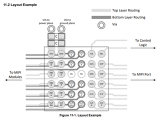
Figure 1 – TMUX646 Layout Example with NFBGA Package Type
This package type is an intuitive design for routing multiple LVDS signals since the differential pins are close together. This makes implementing trace length matching much easier. On the contrary, a WQFN package could potentially make trace length matching more difficult. See that the differential pairs S1A/S2A and S1B/S2B signals are on opposite sides of the package. The LVDS receiver needs to be positioned appropriately in order to have equal trace lengths without having to have serpentine traces.
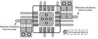
Figure 2 – Layout Example with WQFN Package Type
The below table is a recommendation for multiplexers that can pass LVDS signals on the data signal paths. These devices are controlled via GPIO. The below is not an exhaustive list of all devices that can support LVDS.
|
LVDS Compatible Switches for 1 Transmitter to 2 Receivers |
||||
| Supply Voltage Levels |
Device |
Features | PKG | Dimensions |
|
2.5 V 3.3 V 5.0 V |
1.8-V compatible control inputs Powered-off protection |
UQFN | 10 | 2 mm x 1.5 mm | |
| 3.3 V | TMUX154E |
1.8-V compatible control inputs Power-off protection Supports input voltage beyond supply |
UQFN | 10 |
1.4 mm x 1.8 mm |
| VSSOP | 10 |
3 mm x 3 mm |
|||
|
2.5 V 3.3 V 5.0 V |
TMUX1072 |
1.8-V compatible control inputs Overvoltage protection Powered-off protection Supports input voltage beyond supply |
UQFN | 12 |
1.7 mm x 2 mm |
| VSSOP | 10 | 3 mm x 3 mm | |||