This thread has been locked.

If you have a related question, please click the "Ask a related question" button in the top right corner. The newly created question will be automatically linked to this question.

SN74CBT3244: QSPI signals with 5V supply

Part Number: SN74CBT3244
Other Parts Discussed in Thread: , TXB0304, TXU0104

Hi 
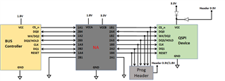
We are using a circuit like shown in the below image.

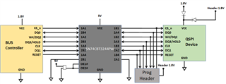
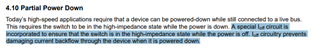
A programming header is provided for programming the device for the first time. A header logic is implemented for OE# to disable the IC, provides isolation between Bus controller and QSPI device during the programming. The 1.8V supply for both controller and QSPI device is isolated so that power from the header will not leak to controller power at this stage. 

As per the datasheet the the SN74CBT3244 supports  " Data I/Os Support 0- to 5-V Signaling Levels (0.8V, 1.2 V, 1.5 V, 1.8 V, 2.5 V, 3.3 V, 5 V).
But on the table "6.3 Recommended Operating Conditions" it is suggested the VIH as 2.0V and VIL as 0.8V
If the VIH and VIL levels specified are applicable to the Input and output pins how it can support 1.8V?

QSPI maximum operating speed 62.5MHz in the fast read mode.

Query 
1. Is the circuit will work? That is can we use the SN74CBT3244 as a 1.8V QSPI buffer?
2. If the VIH and VIL levels specified are applicable to the Input and output pins how it can support 1.8V?
3. In sequence if 5V is coming up first and then 1.8V for Bus controller and QSPI device, is this going to damage any of the Bus controller or QSPI device in a common scenario?
4. Is the SN74CBT3244 will damage if we connect the programmer of 1.8V for programming the QSPI device and SN74CBT3244 is not powered.(5V applied)
5. Is it ok connecting the controller signals everything on the left and device signals everything on the right side? (I can see A and B sides are shuffled in the IC). The current connection shall help in easy routing 
6. If the buffer is not ok for the above purpose please help me to find a suitable buffer IC.

.

  • Hi Manmohan,

    Recall that the simplified schematic diagram for the SN74CBT3244:

    This device is a bus switch. VIH and VIL apply to the control inputs 1/OE and 2/OE. An input signal on 1A1 will show up as output on 1B1 minus a small Ron voltage drop. 

    The inputs and outputs for this device are also overvoltage tolerant, which allows them to go as high as 5.5 V at any valid VCC. 

    1. Is the circuit will work? That is can we use the SN74CBT3244 as a 1.8V QSPI buffer?

    It sounds like you are looking for a buffered solution. The SN74CBT3244 is a bus switch. Are you looking for something to redrive the signal, or are you looking for a device to isolate the signal path?

    2. If the VIH and VIL levels specified are applicable to the Input and output pins how it can support 1.8V?

    This sounds like you are wanting a device that can drive the output. VIH/VIL are logic levels for the control inputs 1/OE and 2/OE, not the voltage levels for the IO paths. 

    3. In sequence if 5V is coming up first and then 1.8V for Bus controller and QSPI device, is this going to damage any of the Bus controller or QSPI device in a common scenario?

    Are you worried about driving signals across the SN74CBT3244 upon using 5V power? This is a bus switch which simply passes a signal I/O from A to B or B to A channel input paths.

    4. Is the SN74CBT3244 will damage if we connect the programmer of 1.8V for programming the QSPI device and SN74CBT3244 is not powered.(5V applied)

    The SN74CBT3244 does not offer powered-off protection. However, the p2p upgrade SN74CBT3244C would solve the back-powering issue because it offers powered-off protection. Is this question similar to question 3?

    5. Is it ok connecting the controller signals everything on the left and device signals everything on the right side? (I can see A and B sides are shuffled in the IC). The current connection shall help in easy routing 

    Are you worried about signal integrity and routing issues? As long as you connect the correct channel paths to your liking you should be okay. 

    6. If the buffer is not ok for the above purpose please help me to find a suitable buffer IC.

    It seems you are looking for a buffered solution to drive your desired output. Let me know if I am understanding your questions properly. I can loop in the appropriate group if necessary. 

    Here is the link to the buffers, drivers, and transceivers product portfolio. 

    https://www.ti.com/logic-voltage-translation/buffers-drivers-transceivers/overview.html 

    Regards,

    Tyler

  • Hi ,

    Thank you very much for the reply.

     1. Are you looking for something to redrive the signal, or are you looking for a device to isolate the signal path?
    Path isolation will be enough for my application. Looking for a bidirectional IC which will provide isolation for the Controller IC while we programming the QSPI Device.

    2. Since in the datasheet its not specified VIH/VIL is for OE i got confused regarding the values. Thank you for confirming.

    3. In normal working condition, 5V for SN74CBT3244 will be coming first and then 1.8V for Controller and Device. Is this going to affect or damage the Controller or Device ICs which is having no power at first (The 5V is from standby supply which will be available all time. 1.8V is available during bootup only.)

    4. No 3 and 4 are two different questions. During programming of the QSPI device, the power shall be provided from the programmer and only 1.8V for QSPI device will be there. During this time the SN74CBT3244 is un powered. So as per your suggestion its better to use  SN74CBT3244C in this scenario which has a power off protection. is my understanding correct?

    5. Each channel is independent to each other and bidirectional right? Suppose i am connecting CS_n on 1A1 and CLK on 2B4, both signal flow is in the same direction. Is this going to create any issue? (Is there any concept like input side like A or output side like B). Since all channels are bidirectional independent channels its should not create any issue. Still for conformation asking the same.  

    6. Re-driver is not necessary. Isolation will be fine. 

  • Hi Manmohan,

    Thank you for your reply. 

    On points 3 and 4, I think the device you would need would be the SN74CBT3244C version. The "C" variant has built in Ioff feature for isolation during power off VDD = 0V. This bus switch can have signals present on the I/O lines while VDD = 0V, without the fear that signals will back power to other down stream devices potentially damaging them.

    The I/Os are bidirectional. "A" can be input/output, likewise, "B" can be input/output. It is 1:1 configuration SPST, so as long as you follow the correct connections for your application below, you shouldn't run into any signal flow issues with the connections you are stating. 

    Example: 1A1 <-> 1B1, 2A4 <-> 2B4. 

    One more thing. It is good to understand that the SN74CBT3244C is a "CBT" device. It uses NFET for the switch so if you are trying to pass signals closer to VDD, you will notice more significant voltage drops.

    Here is an application report describing the differences between CBT-C, CB3T, and CB3Q signal switch devices. Checkout figure 4-2 on page 8. for more of a visual of what I am talking about here.

    https://www.ti.com/lit/an/scda008c/scda008c.pdf?ts=1654627684252&ref_url=https%253A%252F%252Fwww.google.com%252F

    Regards,

    Tyler

  • Thank you very much for the reply.

    My point 3 was a different question

    Suppose my Bus controller and the QSPI device ICs doesn't support power off mode, ie at VDD=0 there should not be any signal on the Input lines.
    The working condition as per now is 5V will be coming first (which is for Bus switch) and then the 1.8V (For QSPI device and bus controller).
    So there will be a state in which only switch will be having the power and not the other two ICs
    In this state is there any chance the bus controller or the device IC will get any signal causing damage of the two ICs? (if i am preferring default ON state for the Bus switch)

  • Hi Manmohan,

    The SN74CBT3244 is a passive device and is not actively driven signals on the I/O lines. If you want to ensure that the internal switches are in High-Z state to prevent any signal from passing through the device, then make sure the appropriate logic HIGH signal is applied to the 1/OE and 2/OE output enable pins. 

    Please let me know if you have any more questions.

    Regards,

    Tyler

  • HI,

    From the Document "CBT-C, CB3T, and CB3Q Signal-Switch Families" its saying the pins will be in high impedance state if vcc=0V.
    VIH for the device is 2V and we are working in 1.8V
    So pulling high when VCC=0V will be difficult.
    So is it ok leaving that open since it wont allow current as per the document 

  • Hi Manmohan,

    Thank you for your question. 

    On page 2. of the SN74CBT3244C datasheet we have the following:

    In order to ensure a high-impedance state between your controller and QSPI device upon power up or power down, you need to tie /OE to VCC through a pullup resistor. Given that the bus switch is connected to VCC = 5V, make sure to tie the /OE pins through a pullup resistor to VCC = 5.0V. This will make sure that even when the device is powered down, it will not allow signals to pass through the bus switch, isolating your controller and QSPI device. 

    Please let me know if you have any more questions.

    Regards,

    Tyler

  • for 1.8V signals with VCC=5V is there any speed limitation with the IC?

  • Hi Manmohan,

    The SN74CBT3244C device has a 200 MHz bandwidth. Signals that exceed the 200 MHz BW margin may experience signal attenuation that could degrade your signal quality.

    Regards,

    Tyler

  • Hi Tyler
    I am planning to modify the circuit like this


    So i am currently looking for a level translator which can change from 1.8V to 3.3V.
    Speed of QSPI clock given as 62.5MHz
    Please suggest a level translator.

  • Hi Manmohan,

    It looks like you are looking for a bi-directional level translator that can support the 1.8V and 3.3V logic levels and pass signals of 62.5MHz frequency. I am looping in the level translating team to take a look at this. 

    Regards,

    Tyler

  • The TXB0304 can support 62.5 MHz (125 Mbps) if the capacitive load is not too high. Please note that it does not work with long traces, connectors, cables, or pull-up/-down resistors.

    For the three fixed-direction signals, you can use something like the TXU0104.

  • What is the maximum preferred trace length?
    Also is there any 6 bit or 8 bit level translator available ?

  • Hi Manmohan,

    For the 6 or 8 CH devices please see TXB0106 and TXB0108. However, note that their data rates as specified in the datasheets are lower from the above TXB0304

    Also, please see the referenced FAQ for the trace length and transmission line effects, thanks.

    Best Regards,

    Michael.

  • There is no fixed trace length limit. The total capacitive load must be smaller than 100 pF, and what trace length this corresponds to depends on the board characteristics. Anyway, shorter traces improve signal quality.

  • Longer trace length will increase the load capacitance and will be decreasing the speed right?
    Any other drawback is there with longer trace length ?

  • If the capacitance is too high, the TXB's edge accelerators will time out before the output voltage has reached VCC/GND.