What is Charge Injection?
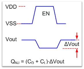
Charge injection (QINJ) is the coupling of the switch control signal through some parasitic capacitance. The charge present from this parasitic capacitance is then injected into the switch / multiplexer output. Charge injection is a very important parameter for fast switching applications. As the signal frequency becomes faster, the charge on the output node has less and less time to discharge the leftover charge from the parasitic capacitance. Thus, affecting the output voltage more significantly as frequency increases. Another way to think about this is that an increase control pin frequency, more of the control pin will “bleed” through the parasitic capacitance to the output (see Figure 2).

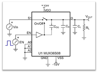
Figure 1. MUX36S08 Charge Injection Model

Figure 2. MUX36S08 Output Effected by Charge Injection
The gate-to-drain parasitic capacitance of the internal switch is responsible for excess parasitic charge coupling onto the output of the signal. This toggling of the control pins (EN, Ax, or SELx) from LOW to HIGH couples some of this signal through CDG onto the output VOUT.
Charge injection is a factor of the drain parasitic capacitance of the switch (CD) and the load capacitance (CL). This is represented by the equation below:
QINJ = (CD + CL) x ΔVout
Equation 1. Charge Injection Equation
Note in equation 1 above, increasing the load capacitance CL will minimize the change in output voltage ΔVout due to charge injection. However, as you increase load capacitance, be aware that this will directly affect the bandwidth of your output system due to increasing RC characteristics.
A smaller CDG will also reduce the amount of charge injection in the analog switch / multiplexer, however, this mostly depends on the topology used internally to the device. Usually, devices that contain larger on-capacitance (CON) will introduce worse charge injection.
Devices with low charge injection:
| Device | Charge Injection (pC) |
| TMUX6111 | 0.6 pC |
| MUX36S08 | 0.3 pC |
| TMUX1574 | 3.5 pC |

