Other Parts Discussed in Thread: TMUX136
Hi team,
Let me clarify the issue, When we popular TS3DS10224.in the circuit. as you can see the eye diagram measurement result cannot pass the USB2.0 compliance test requirement.
But, if we bypass the TS3DS10224 ( using external cable to short the traces on the PCB pads), the eye diagram can pass the USB2.0 compliance test requirement. That prove the PCB design is no problem.
Questions.
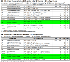
1. What's the internal impedance (Z) of TS3DS10224 pins (both input and output pins)?
2. Is there other parts we can alternative TS3DS10224 to get better performance? pin to pin is better.
3. Any recommendation about TS3DS10224 at USB2.0 application?
Muhsiu