This thread has been locked.

If you have a related question, please click the "Ask a related question" button in the top right corner. The newly created question will be automatically linked to this question.

TS3A27518E: TS3A27518ERTWR for switching gigabit network signals

Part Number: TS3A27518E
Other Parts Discussed in Thread: TS3L501E

Hi, 

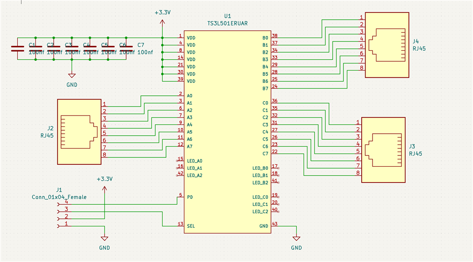
I want to create a module based on TS3A27518ERTWR to switch b/w two networks. Network may be 10Mbps, 100Mbps or 1000Mbps. The idea is to connect three RJ-45 connectors to multiplexed pins as shown below:
I have the following questions:

  1. Can it be used to route 10Mbps, 100Mbps or 1000Mbps signals from Ax pins to two different targets (connected to Bx, Cx pins)?
  2. Any obvious problems with above schematic?
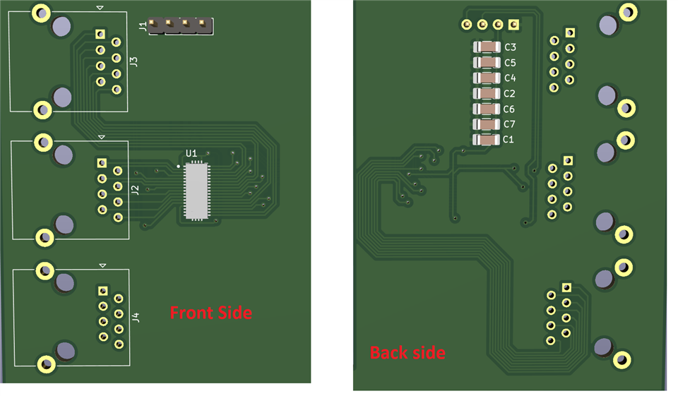
  3. The traces are routed as below, is there a problem with these routing. I mean in the Network cable, there are 4 pairs of two two wires (total 8 wires) but on PCB should these pair wires be kept close to each other or plan 8-wires are fine as shown below.
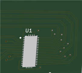
  4. There are few vias, that I cannot avoid, will they be problematic?
  5. The traces width is 0.25mm which should be increased a bit?
Thanks in advance.

Waiting for the recommendations.

  • The concept you are working on makes sense to me. I have a few concerns/suggestions. 

    Just to confirm are you using the TS3A27518E or TS3L501E? The post says TS3A27518E but the schematic has a TS3A27518E. 

    Please keep in mind that the bandwidth of the TS3A27518E is 240MHz. So you may limit your data rate, particularly on the 1000Mbps through the switch. The TS3A27518E has a much higher bandwidth at 600MHz which will likely reduce the losses through the switch quite significantly. 

    The trace routing you have may be ok, but the traces in parallel could cause AC coupling and lower your highspeed performance. Vias will impact your AC performance but sometimes they are unavoidable. It can be hard to know their true impact without a PCB level simulation. Trace width is not as important in this type of application as the overall trace impedance. Which will determined from from the PCB material, dielectric thickness, and trace width. 

    Please see TI's application note on highspeed layout guidelines for the most comprehensive inputs on your layout. This will have much more information on the best ways to layout and route your high speed signals. 

    https://www.ti.com/lit/an/spraar7i/spraar7i.pdf 

  • Hi, 

    Thanks for the reply. My apologies for the part number mistake. I am using TS3L501E. You have given a detailed reply but unfortunately I could draw any conclusion. So still same questions:

    Will the switching circuit work probably?

    How I can avoid AC coupling you mentioned for the parallel lines.

  • Hi

    I can't guarantee that your board will work, you would have to run some PCB level simulations for that which TI doesn't support through this forum. Based on your schematic, you system should work electrically, but please keep in mind best practices for high speed routing to ensure the best possible performance. The best guidance on the PCB would be in the application note I linked above. 

    To avoid AC coupling the best thing you can do is space out signals that may interfere with each other, such as conflicting data lines, or clock lines. And keep any differential pairs close together to ensure proper differential trace impedance. 

  • Thank you so much for the reply. I have already separated and combine differential lines. All I want to know if the IC can be used for switching network of various data rates e.g. 10,100,1000 Mbps.

  • Yes, the TS3L501E can support 10, 100, and 1000 Mbps Base-T signal switching as per the datasheet. Just note figure 6-1 on any losses you may have through the switch at the higher data rates.