This thread has been locked.

If you have a related question, please click the "Ask a related question" button in the top right corner. The newly created question will be automatically linked to this question.

CD4053B: Signal waveform problem

Part Number: CD4053B
Other Parts Discussed in Thread: TMUX7436F

Hi team,

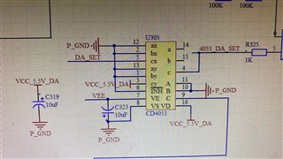
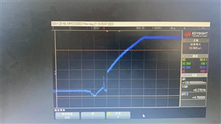
When use the CD4053 for signal selection, but at power up instant, the output signal waveform is undershooed for a while. 5.5VDA is selected by default at power-on. Below are the Sch and signal waveform. What's the reason for that ?Thanks for your response.
  • Hello Enhui!,

    For my understanding I want to clarify what you are seeing in your design. 

    1.Are you passing as signal through your device at the same time you are powering up the devices vcc supply?

    2. What is the voltage of the signal in between the two yellow lines on your second picture?

    Please let me know these things.

    Regards,

    Kameron 

  • Hi Kameron, 

    Thanks for your comments, below is the response about your questions.

    1. Yes.

    2. 4053_DA_SET. VEE= -7.5V, VEE and VCC -5.5V-DA are almost the same time to rise when powered up.

  • Hi Kameron,

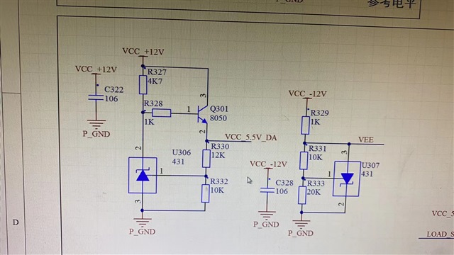
    Below is the power supply of CD4053.

  • Hello Enhui,

    1. I think the reason you see the problems with this design is because this device doesn't have a feature called power off protection. This feature makes sure that unintended signals do not pass through your multiplexer when the signal input has a voltage on it before the power supplies of the device VDD. (This a possibility in your design).

    2. I think the best device we have with power off protection that can support 5.5v and -7.5v signals is the TMUX7436F.

    3.Also you could you please tell me more about this business case

    Please let me know if you have any questions!

    Regards,

    Kameron