


Hi TI E2E design support team
While I was choosing appropriate Mux for my system, I got a question regarding powered off protection.
Since SN74LVC1G3157DSF doesn't recommend to apply any signal to input when there's no VCC due to its clamping diode, I was planing to use TMUX154e because of powered off protection function.
However, I couldn't find detailed information or logic about powered off protection anywhere else than its title.
What I only assumed about protection function is that TMUX154e still has parasitic clamping diode but EN pin is doing something with it.
Then, of course, another question comes up to me how EN logic can work when there is no supplying voltage.( maybe that's why it's logic low active pin ?)
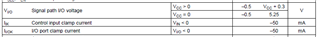
Hope I can get elaborated info about Powered off protection and can assure the situation like some signal is applied to input pin when there's no VCC.
If i'm missing anything from the datasheet please let me know.
Thanks

