This thread has been locked.

If you have a related question, please click the "Ask a related question" button in the top right corner. The newly created question will be automatically linked to this question.

TS5A23166: No high impedance with floating VCC( Isolation in Powered-Down Mode vs Power off Protection)

Part Number: TS5A23166
Other Parts Discussed in Thread: DRV8701,

Hello,

I finally used the TS5A23166DCUR for the application but it don’t run as I thought….

I have the schematic of the figure.

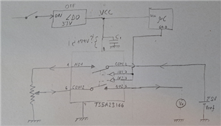
With 2,5V in Vref, if the LDO turn off, VCC should be 0V, but I have around 1,29V… and this voltage varies with Vref  (in COM1). If Vref is less than about 1,9V, then VCC is about 0,7V and below of this Vref value, Vcc goes to 0V and the TS5A23166DCUR switch off correctly.

It appears that the voltage of COM1 >2V drain to Vcc and supply the TS5A23166DCUR.

I was hoping that with ldo off, TS5A23166DCUR goes to high impedance. What could be happening?

Thank you!

  • Hello Ger.,

    Happy to help solve this problem with you!

    1.With 2.5Vreff and LDO off , signal path from com1 and no1 should be off hi z. Power off protection only applies on the signal path. If the device is accidently powered on (from the supply voltage setup ) you have above, then power off protection will not be activated for this device. 

    2.Device has no esd path from (inputs or outputs) to supply, so VCC shouldn't change at all based on inputs.

    My idea is that the capacitor and LDO is supplying some voltage after you turn the LDO off/ disconnect it.

    Let me send this to the LDO team and see if they can help here!

    Regards

    Kameron

  • Hello Ger.,

    If this is an LDO made by TI, can you let us know what part number it is?  Otherwise we won't be able to offer any support regarding the LDO.

    Thanks,

    Stephen

  • Hello Kameron!

    Thank your for you answer.

    The LDO really is the LDO of the driver DRV8701 (DVDD), but I don’t thing that it is important.

    To simplify the circuit, I have put a switch between the LDO output and the TS5A23166.

    - Vref always with 2,5V

    - With S1 closed and S2 Closed all run fine.

    - With S1 Open (really driver off) the voltage in A=B= 1,29V

    - Then, if I open S2, the voltage of A=0V and the voltage of B=2,065V ¿?

    There isn’t else connected to the point B. Only C1 and the Vcc of TS5A23166.

    If, in this situation, I lower Vref, then this Voltage also goes down. For example, if Vref=1,8V, then VB=1,4V. if Vref=0,9 then VB=0,5V…

    ¿Why?

    But, in this situation, if I low Vref to 0V and  then I increase the Vref until 2,5V, then, it run ok. VB keeps 0V and COM-NO are in high impedance at all times.

     I think that If I switch-off VCC when Vref=0, the behavior is as expected (high impedance), although later Vred increases. But if I switch-off VCC when Vref>1,5V then TS5A23166 it feeds itself. I can't find any other explanation…

    What does you think? I understand that this should not be like this. Correct?

    Regards

  • Hello Ger,

    I think we should look into the  idea that the capacitor is storing charge  and keeping a voltage on the vcc pin of the mux even when you switch off s2.

    If the voltage on vcc is never zero, then you will not see the hiz power off protection signal path you are looking for.

     I think that If I switch-off VCC when Vref=0, the behavior is as expected (high impedance)

    This is basically having a 1.29v supply on the mux and having no input. so the device will have a high z signal path.Having a supply not in the range of 1.65 to  5.5v is not recommended for this device.

    But if I switch-off VCC when Vref>1,5V then TS5A23166 it feeds itself

    In this situation you basically have the mux with a 1.29v supply and signal greater than 1.5v on the io/ signal pin. This is not recommended for this device.

    I think Stephen can help better about the  actual discharging of the capacitor. I think there is a connection between the Ldo and the capacitor needing to discharge.

    What do you think about this information?

    Please let me know!

  • Hello Kameron!
    The capacitor is only a bypass 100nF as advice the datasheet.
    I understand that for a short period of time, the capacitor supply the TS5A23166, and this have a indeterminate state, but the capacitor can’t to be suppling permanently 1,29V... This voltage come drained from something and only the TS5A23166 is connected with S2 open.
    Anyway, I have removed the capacitor to prove, and have the same behavior.
    Is it sure that the TS5A23166 switch to high impedance if switch off VCC, having still voltage>0 on COM1/2 or NO1/2?
    Regards

  • Hello Ger,

    Ok understood,

    I will move this back to the mux thread so we can resolve this there.

    1. Can you try to test the device  with  vcc pin of the mux grounded  and  having voltage>0  on the NO1/2 or COM1/2 or NO1/2. I think the floating supply may be a problem here.

    2. can you try to use  another TS5A23166 when you test again.

    Lets see if it still behaves the same after this testing 

  • Hello Kameron!

    I’m a bit confused… If you remember, I remobed the capacitor in the last test. Today I going to grounded the VCC as you tall me, but now I see that if I open S2, then VB is 2,065, but the voltage on NO1now is 0V (now, if I turnoff the LDO, then NO1=COM1, but if then I open S2, then NO1=0, although VA it keeps 2,065V). I don’t know why this has change… But I’m sure that before if I opened S2, then was kept NO1=COM1. I have put the capacitor, but the behavior is maintained.

    Anyway, if the Ldo is off, NO1 shouldn’t are equal to COM1.

    Answering your questions:

    1. If I ground Vcc, (VB=VA=0V) the TS5A23166 turn to high impedance. If I remove the grounded, everything remains the same (high impedance).
    2. With another TS5A23166, happened the same in all cases


    I have done other test. I put a ammeter. With the LDO off, 1,4mA go from VB to VA.

    Then if I put a rectifier diode (anode VA, cathode VB) then all run fine!  This could be a solution for mi application because Vcc is 3,2 and the signal are lowet that 2,5V, But I think that it shouldn’t be necessary…


    what do you think?

  • Hello Ger,

    but if then I open S2, then NO1=0, although VA it keeps 2,065V

    1. The mux is unpowered in this scenario and has a hiz signal path.

    I don’t know why this has change… But I’m sure that before if I opened S2, then was kept NO1=COM1. I have put the capacitor, but the behavior is maintained.

    2. Good to hear this part of your issue is resolved! 

    I agree that your diode solution should not be necessary. This is  because this device has power off protection which means there is supposed to be no path from any of the io pins to supply. So the 1.4mA going from VB to VA should not happen. Can you double check your setup and confirm you are seeing that current with multiple TS5A23166?

    Also in your current setup if your mux is seeing a supply voltage of 1.29V  at any point  and if you have a signal on the io pins your muxes could be getting damaged. 

    Please let me know the results of the re -testing and we can try to figure this out.

    Regards


  • Hello Kameron!

    I have now two TS5A23166 and about 1,4mA goes from B to A on both. I will try with two more this week.

    As told you, if I grounded this point an instant, then this current goes to 0mA and stays there.

    I have confirmed it with production department, and the reference placed on the prototypes is TS5A23166DCUR.

    Regards

  • Hello Ger

    ok understood please let me know the results of that testing.

    So i have more questions about the condition with LDO off and s2 connected(when you are seeing 1.4ma)

    1.when you see 1.4ma form vb to va, what is the vb/va voltage?

    2.What are the voltages of all the signal pins for the device. No1,No2, COM1, COM2?

    3. is there any current going into the signal pins of this device that could be providing the 1.4ma?

    After talking to the design team, there might be devices with better power off protection for your application with( floating supplies instead of zero volts) or you could use the solution that you created with the rectifier diode.

    Please let me know what you think.

    Regards

  • Hello Kameron,

    1.when you see 1.4ma form vb to va, what is the vb/va voltage?

          1,32V

    2.What are the voltages of all the signal pins for the device. No1,No2, COM1, COM2?

         - COM1=2,5V(in)

         - No1=2,5V(out),

         - COM2=1,4V (in) it depend of the potentiometer position

         - No2= 0,16V ¿? (out)

    3.is there any current going into the signal pins of this device that could be providing the 1.4ma?

         Yes Vref on the COM1 pin and the return of this in COM2

    Really, the application haven’t floating supplies. Only the VCC(LDO) switch off and it should to be 0V. I have put S2 only to find out what happens.

    The diode is a solution for me, but I have to re-design the PCB… and I have 50 PCB made. If there is a better alternative with the same footprint and pinout, I’m interested.

    Regards!

  • Hello Ger,

    Ok I understand more now so thanks. 

    Basically this device's power off protection works  when vcc=0v exactly.

    With this device, if the voltage on its supply is not exactly zero  and the signal on the input is higher than the supply,  a  path will be created  from  the signal pin to the supply where current can go up through the device.

    We do have devices that can support  power off protection for  your specific  application and should not need the external diode solution. 

    1.SN74CB3Q3305DCUR - It has the same package but different pinout than your current device, also the supply current for this device is higher than the device your are using now

    2.The SN74CBTLV3126PWR is a 1:1 4 channel device but can also support the power off protection needs for this application.

    Finally your diode solution is fine and but if you want to look into these other devices i have here please let me know!

    Regards

  • Hello Kameron,

    OK, thank you. I will study these chips.

    But I don’t understand… I understand that if something external to TS5A23166 keep 1,3V in VCC pins, then the problem occurs. But it is the TS5A23166 itself that causes the 1,3V on Vcc pins... How useful is the power protection on this chip? will it only do it when the voltage nox=comx=0? His behavior is strange and confused.

    Regards

  • Hello Ger 

    For this device the power off protection circuity will only activate if the vcc=0v . Because in this design vcc is not strongly pulled down   to ground there is a current path from the input signal pins to the supply of the mux.( Please remember this for this device)

    For example if you pulled node b down to ground . This device would have 0v on its supply and the power off protection would activate.

    I understand the confusion, so to clarify there are other devices that have power off protection that will activate at supplies of 0v and at supplies that are not strongly pulled down to ground. The two devices I suggested earlier would  work better in this application and do not need the strongly pulled down to ground supply to have there power off protection circuitry activate.

    I understand the confusion, this device does have power off protection and is reliable. The power off protection (when activated) can block signals  0v to vcc.

    Please let me know if this helps answer your question. 

    Regards

    Sincerely 

    Kameron 

  • OK Kameron!

    Thank you very much. Delighted to speak with you

    Regards