This thread has been locked.

If you have a related question, please click the "Ask a related question" button in the top right corner. The newly created question will be automatically linked to this question.

TMUX1308-Q1: Injection Current Control

Part Number: TMUX1308-Q1


Tool/software:

Hi team,

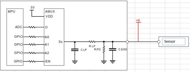
Our customer has some questions about injection current control in TMUX1308-Q1. They want to understand this function can work to protect Source pin when it is short to 12V battery.

(Expected use case)

Questions:
1. Please confirm the behavior when an overvoltage is applied to the Sx pin of the device. Our understood that when overvoltage is applied to the Sx pin, the FET in injection current circuitry is turned on. As result, output from D pin will be around 0V. Is the understanding correct?
2. If the understanding of #1 is correct, our understanding is that the voltage of the Sx pin is the voltage divided between the RLIM (external series resistor) and injection current circuitry FET rdson. Please tell us the min and max values of Ron of FET.
3. The output voltage from D pin will be around 0V in the above use case. Is that correct? 

4.  What are the conditions for the FET to turn on and turn off for overvoltage protection? Could you provide the min/max value and hysteresis voltage for turn on/turn off thershold?

5. For example, considering the case where the S2 pin shorts to battery while S1 pin is selected. Will there be any influence on the D pin? If so, please tell me how to calculate the voltage that affects D pin.

Thank you,

Muwei Zheng

  • Hello Muwei,

    Please see answers below: 

    1. Yes, you are correct. When there is an overvoltage event on the I/O pins, the injection current control will trigger and won't let the signal pass through the switch, resulting almost 0V on the drain side. 

    2. The voltage on the Sx pins during injection current control is related to your VDD. In your case VDD  = 5V, so the voltage on the source pins will be a bit above it approximately 6V. 

    3. Yes, that is correct. The signal won't pass through the switch, due to the current being directed towards the FET and on the drain side you will see voltage ~0V.

    4.  It will turn on if an input voltage (VIN) higher than the positive supply (VDD + ∆V) or lower than ground (VSS). It will turn off if the signal doesn't exceed above the supply, or below ground. 

    5. There will a small insignificant influence on the D pin. Your will see the signal from your selected source on the drain side with very minimal disturbance. This is related to the crosstalk parameter, which is very low for this device.

    Thanks,

    Nir 

  • Hi Nir,

    Thank you for your quick response! I have a few further questions:

    2. The voltage on the Sx pins during injection current control is related to your VDD.

    Could you help elaborate more about how injection current control circuitry works to clamp Sx pin voltage? Does this IC has internal voltage monitor and control the pull down resistance based on Sx voltage? How should we calculate the clamp voltage?

    4.  It will turn on if an input voltage (VIN) higher than the positive supply (VDD + ∆V) or lower than ground (VSS). It will turn off if the signal doesn't exceed above the supply, or below ground. 

    Where does ΔV come from? Is it possible to provide the min/max variation of the detection threshold?
    Are there hysteresis characteristics in turn on and turn off threshold or just the same?


    Thank you,

    Muwei Zheng

  • Hello Muwei,

    For the injection current control circuitry to be active, two conditions must be present. First, the voltage at the source or drain pins is greater than VDD, or less than GND. Next, the channel must be unselected. With those  two requirements met, the protection FET will be turned on for any disabled signal path and shunt the pin to GND. The clamp voltage is 0.5V above the supply.

    ΔV comes from when there is an overvoltage event on an unselected pin. The detection threshold is usually around 0.5V above the supply.
    We don't have information on the hysteresis characteristics of the turn on and turn off threshold, but I would assume they are the same.

    Thanks,

    Nir 

  • Hi Nir,

    Thank you and I understood the injection current control active condition. I have a few further questions:

    1. As you mentioned detection threshold is VDD+0.5V. For example, if VDD=5V and unselected Sx input is 5.5V, will the drain output being chattering between 5.5V and 0V, since there is no hysteresis characteristics?

    2. For crosstalk calculation, is it correct that drain output will be the multiply of selected source voltage?

    For example, if VDD=5V, S0=3V, S1=9V and S1 is selected,

    20*log(Vout/3) = -110, so D pin voltage will be around 0.012V?

  • Hello Muwei,

    1.After confirming with the design team I realized I was wrong. You will still see voltage on the drain side.
    Meaning for example if your VDD = 5V and on the source side is 5.5V, what you will happen is the following:

    - The injection current control will activate 

    - You will see ~6V on the source side and ~5.5V on the drain side.   

    2. It will not be a multiply, but the more selected sources you have the greater the crosstalk is. 
    The calculation is incorrect, following that equation; the voltage on the drain pin will be ~0.00001V.

    Thanks,

    Nir 

  • Hi Nir,

    Let me double check, drain voltage will be VDD + 0.5V + crosstalk voltage, when the unselected Sx pin voltage is above VDD+0.5V?

    Also, if the selected Sx pin voltage is above VDD+0.5V, drain voltage will be same as VDD + 0.5V + crosstalk voltage?

  • Hello Muwei,

    Yes, that is correct; but as shown earlier the crosstalk voltage is very low and not substantial . 

    Drain voltage will be a bit lower than VDD + 0.5V + crosstalk voltage. Meaning, the voltage on the drain side will be lower than the voltage on the Sx side.  

    If you are seeing 6V on the Sx side, you will probably see ~5.5V on the drain side. 

    Thanks,

    Nir 

  • Hi Nir,

    Thank you for confirmation. I just have one more follow up question.

    1.After confirming with the design team I realized I was wrong. You will still see voltage on the drain side.
    Meaning for example if your VDD = 5V and on the source side is 5.5V, what you will happen is the following:

    - The injection current control will activate 

    - You will see ~6V on the source side and ~5.5V on the drain side. 

    So in this case even if the selected Sx pin is lower than 5.5V, we will still see ~5.5V on the drain side when injection current control activate? Is it because drain side is also clamped to VDD?

  • Hello Muwei,

    I can't confirm the behavior when the signal is on the Sx is lower than 5.5V, because it is exceeding recommended operating ratings, but might not trigger the injection current control. This state is unknown and I can't guarantee device behavior.  

    What I can confirm is during normal operation (no voltage signal is exceeding recommended specs) when a selected switch has a signal voltage sent to it, the drain side will see similar voltage level. During an injection current control event you will also see voltage on the drain side, but a bit lower than on the source side. 

    There is no diode to VDD.

    Thanks,

    Nir