This thread has been locked.

If you have a related question, please click the "Ask a related question" button in the top right corner. The newly created question will be automatically linked to this question.

SN74LV4052A: crosstalk issue when there are 1.5V DC signal in 8x ch

Part Number: SN74LV4052A
Other Parts Discussed in Thread: TL074

Tool/software:

Hi Ti experts,

My customer uses TL074 + SN74LV4052 for current sensing. They use two-stage TL074 for current amplification and voltage follower. Then they use all the 8x input channels on SN74LV4052. 

Now all the 8x input signals for 4052 is 1.5V DC from TL074 when channel current is 0A. Current level is from -40A to +40A and Accordingly TL074's output is from 0 to 3V.

Issue is that when all the 8x channels have 1.5V DC input. Output signal will have 0V/1.5V and 3V output. Noise will also affect the input signal. There will be a 200mV step on 1.5V input signal.

1. TL074 schematic

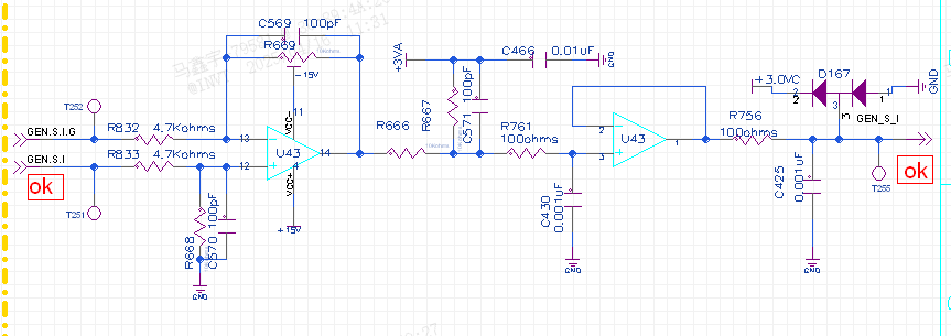
2. SN74LV4052 schematic

3. MUX's power supply

4. PCB layout

5. Testing results for only one channel input and output.

Green signal is input signal and yellow signal is the output signal.

6. Below are three input signals and one output signal

Yellow signal is the output signal.

I have several doubts:

  • Two SN74LV4052 are put on the bottom of PCB. There are 6 layers. Top, GND, Signal, Signal, Power, Bottom, which means there are no complete ground plane under the SN74LV4052;
  • Is 3.3V power supply for SN74LV4052 suitable for 0 to 3V input signal range;
  • Is the issue relevant to software. You can see in last picture. Yellow signal have a 2s period. Could you please share the software control logic for SN74LV4052. 

Below are the software setting for SN74LV4052.

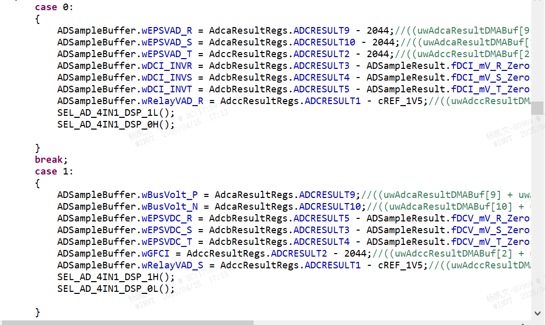
From their software engineer, they will switch the 4:1 mux and sampling for 1ch signal in 52us. They need 

  • Hi Gary,

    • Two SN74LV4052 are put on the bottom of PCB. There are 6 layers. Top, GND, Signal, Signal, Power, Bottom, which means there are no complete ground plane under the SN74LV4052;-
      • It looks as if the device is gnd properly based of the schematic so that should be fine
    • Is 3.3V power supply for SN74LV4052 suitable for 0 to 3V input signal range;
      • Yes this device can pass 0 to 3V signals when the supply is 3.3V
    • Is the issue relevant to software. You can see in last picture. Yellow signal have a 2s period. Could you please share the software control logic for SN74LV4052. 
      • The Sn74LV4052 doesnt have software to control it. It is a analog multiplexers that is controlled by High and Low signals sent to its control pins

    So to help debug this system I wanted to ask you some more questions 

    Are you saying that when 1.5V is on all the input pins of the multiplexer that 0V,1.5V and 3V are all voltage readings that you are seeing on the output pins COM1 and COM2?

    For example are you saying there is 1.5V signal on the input and 3V signal on the output com pin( This shouldn't happen but please let me know)

    In addition can you share scope captures where we can see the input signal, output signal and changing of the control pins/( probing input output and control pins)

    Please let me know and regards,

    kameron 

  • Hi Hill,

    • Is the issue relevant to software. You can see in last picture. Yellow signal have a 2s period. Could you please share the software control logic for SN74LV4052. 
      • The Sn74LV4052 doesnt have software to control it. It is a analog multiplexers that is controlled by High and Low signals sent to its control pins
        • I mean software control logic rather than software like 1. select channel1 by option pins; 2. open IC enable; 3. ADC sampling; 4. time delay; 5. close IC enable; 6. select channel 2; 7 open IC enable; 8. ADC sampling;
        • Do you have a software control logic guidance? I think it is important to avoid corsstalk.
    • Are you saying that when 1.5V is on all the input pins of the multiplexer that 0V,1.5V and 3V are all voltage readings that you are seeing on the output pins COM1 and COM2?
      • Yes. 
    • For example are you saying there is 1.5V signal on the input and 3V signal on the output com pin( This shouldn't happen but please let me know)In addition can you share scope captures where we can see the input signal, output signal and changing of the control pins/( probing input output and control pins)

      • ok. I will add the picture of the change of control pins.
  • Hi Gary,

    1.I actually do not have experience programming systems to control adc sampling  and I can only give guidance on how to control the multiplexer with the logic table of this device. Could  you explain more about what you mean by crosstalk?

    2. Could you please send a waveform of this happening? For example can you show me 1.5V being placed on the input of the mux and 3V on the output. 

    Maybe probing the io pins and recording a scope shot of 1.5V on the input pin of the mux and 3V on the output  piin of the would help( This shouldn't happen but please let me know and I can think more about this)

    3. In addition I think you might have forgot to add the control pin scope shots but those will also help.

    Happy to help debug here and see if the issues is the multiplexer in this application

    Regards,

    Kameron