This thread has been locked.

If you have a related question, please click the "Ask a related question" button in the top right corner. The newly created question will be automatically linked to this question.

TXS0108E: Switching time between A to B and B to A

Part Number: TXS0108E

Tool/software:

Hi, 

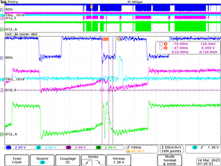
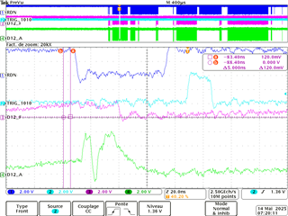
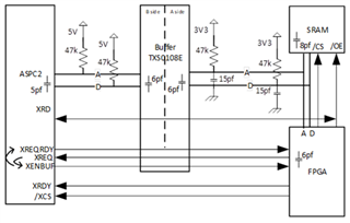
in my design I currently use buffer bi-directional TXS0108E without direction control signal.

On side VCCB I have an ASIC powered in 5V and on the VCCAr side a FPGA + SRAM powered under 3V3.

Each side there are 47k-ohms pull-up resistor.

I would like to know how many time to wait between sending data from A side to B side the B side to A side, I can fing only propagation time in datasheet.

Thanks for your feedbak, 

Regards

Denis

  • Hi Denis,

    Can you provide more information of the interface of signals that this question pertains to? TXS0108E supports open-drain and push pull drivers, and the device itself has open drain outputs with internal pullups- the default state is logic high and dominant state is logic low when either side of the bus is driving. Care should be taken to not have A/B side driving opposite states as this would lead to bus contention issues. 

    Regards,

    Jack

  • The TXS has internal pull-up resistors; you do not need external ones.

    The TXS is not a buffer; the pass transistor works as a passive switch. When any of the two sides is pulled low by an external device, the switch closes, and the other side is pulled low, too. There is no minimal time to switch directions; it would be allowed for both sides to pull the line low at the same time.

  • Hi Jack, 

    B side there is an ASIC component (ASPC2 5V) with 47k external pull up on each adress/data signals. 

    A side there are a FPGA and SRAM powered in 3V3.

    In normal operating mode, ASPC2 read/write data from/to SRAM through buffer TXS0108E, then sometimes, FPGA (A side) write and read data in SRAM which is also A side.

    The ASPC2 chip select is driven directly by FPGA through 3V3 signal (compatible with CS/ in TTL 5V from ASPC2) to ensure ASPC2 adress/data are in HZ when FPGA read /write SRAM.

    I had saw in application not that 47k-Ohms external pull-up resistor can be used A side and B side.

    Thanks for your feedback

  • In our design it is a good parctice to avec external pull-up resistor and this value (47k) is allowed as defined in document scea054a.pdf.

    Our bus operating frequency is 15.625Mb/s.

    "There is no minimal time to switch directions" -> Is there maximal time to switch direction ? I mean if B side there is a component wich is unselected (in HZ) , so due to pull-up soem signals can goes from low to high and is this case is transistion low to high can be detected by TX components and this component can force A side a high level during 30ns ? even if B side SRAM memory impose low level ?

    Thanks

  • Isn't the SRAM connected to side A?

    Assuming that both SRAM and ASIC are driving the line low, and then the ASIC goes inactive, then the lines on both sides stay low.

  • Yes SRAM is connected A side. In our application FPGA (A side) read a high level instead of low level SRAM side (which is also A side)

  • Please show an oscilloscope trace of the signal on both A and B sides.

  • Blue dark RDN: signal which manage SRAM and ASPC2

    Pink D12_F: data12 FPGA side

    Green D12_A: data 12 ASPC2 side

    Blue light TRIG_1010: signal managed by FPGA to trig failure

    My understanding is if last data value state is low level, and the all bus are set in HZ (both side), due to pull-up and parasitic capacitors, signal will goes from low to high slowly up to low to high transition is detected by the buffer (whatever the side).

    Is transition is detected on side (ASPC2 side for example), so on the other side (SRAM side) state high is imposed during I guess close to 30ns, but during this time, if SRAM impose also low level, there is a bus contention.

  • The edge accelerators trigger when they detect the beginning of a rising/falling edge, which happens at about 30%/70% of the respective VCC.

    The voltage on the 3.3 V side is not a valid low level. The pull-up resistance does not change; the only reason why the voltage would creep up is because the device that pulls low (SRAM or FPGA?) reduces its drive strength, or because the SRAM and FPGA try to drive the line to different values.