Tool/software:
Dear TI team,
We are planning to use the TMUX121 in our design and would like your confirmation on the following points:
Design Requirements:
DAT0, DAT1: 104 Mbps single-ended signals (from SD 3.0 interface)
CLK_P, CLK_N: 100 MHz differential PCIe clock (HCSL signaling)
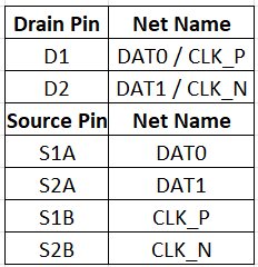
The above table is reference for signal connections by using TMUX121
-
When SEL = 0 → D1/D2 are connected to S1A/S2A (SD 3.0 mode)
-
When SEL = 1 → D1/D2 are connected to S1B/S2B (PCIe mode)
Questions based on our design requirements:
-
Can the TMUX121 support 104 Mbps single-ended signals on the source and drain pins?
-
Can The TMUX121 handle a 100 MHz differential ended PCIe clock (HCSL) on the source and drain pins ?
-
Are the source and drain pins compatible with 1.8 V I/O levels?
Note: Request you to revert back at the earliest