


Other Parts Discussed in Thread: TCA9535, TCA9803
Tool/software:
Hi,
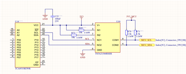
I am designing a system where a slave I2C device will be powered down while the master is still on. Therefore, I need to isolate the slave from the I2C bus and the TS5A21366 looks suitable.
My question is about the power on/off sequence of the device. The 3V3 power supply (SMPS) will be shutdown by an external enable signal from the master device (MCU). Will the setup in the schematic below work? I'm concerned that as the device is powering down (3V3 approaches 0V), the switchs will remain on and 3.3V from the I2C bus will remain on the slave I2C pins until the TS5A21366 switches off. Would this damage the TCA9535? In the TCA9535 datasheet it says "For voltages applied above VCC, an increase in ICC results."
Another option is to connect the 3V3 external enable signal to the IN1 and IN2 pins so that the TS5A21366 switches are disabled at the moment the 3V3 regulator is switched off. However, when the 3V3 is switched back on, IN1 and IN2 will go high before the V+ pin is brought up to 3V3.
Datasheet: "To avoid an increased quiescent current (ICC) condition, proper power sequencing must be followed to ensure that the bias circuitry is powered up prior to applying voltage on the I/Os. The proper sequence is for the VCC pin to be brought up to VCC before the control inputs (IN1, IN2) are allowed to go to a high level."
With the setup in the schematic, would this also be an issue as the IN pins are powering up at the same time as VCC?
Also, the master(MCU) is on a seperate PCB via an FPC and 3V3_MCU is not avaliable on the PCB with the slave device, so devices like the TCA9803 would not be suitable.
Looking forward to your response and hoping we can come to a decisive conclusion as this has to work first try.
Thanks,
Austen


